
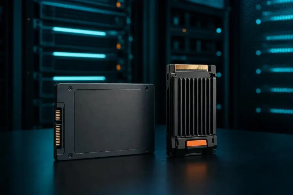
In the rapidly evolving landscape of data storage, the terminology used to describe modern hardware often leads to a fundamental misunderstanding of how technology actually functions. For many consumers and enterprise IT buyers, the terms "Flash" and "SSD" are used interchangeably, yet they represent two distinct levels of a complex technological stack. Understanding the relationship between the raw memory medium and the finished storage product is no longer a matter of semantics; it is a prerequisite for making informed purchasing decisions in an era where data speed and reliability define the limits of computing performance.
Flash storage is not a device in itself, but rather the underlying memory technology—a collection of electronic chips designed to store data using no moving parts. A Solid-State Drive (SSD), by contrast, is a sophisticated, integrated device built around those chips. According to industry leaders like IBM, an SSD is a complete ecosystem that includes a controller, specialized firmware, and a standardized interface. While they are often discussed as if they were competing options, they are actually complementary components of a single architecture. The real challenge for modern buyers lies in navigating the specific variables within that architecture, such as NAND types, interface protocols, and endurance ratings.
Flash Is the Chip, SSD Is the Product Built Around It
The distinction between the raw material and the finished product is the first hurdle in understanding modern storage. Flash storage refers to non-volatile electronic memory chips that retain data by storing electrical charges in memory cells on silicon. Because these cells do not require a constant power supply to keep their state, Flash is the ideal medium for everything from the smallest USB thumb drives to the massive storage arrays found in enterprise data centers.
However, as Pure Storage emphasizes, the presence of Flash memory does not automatically make a device an SSD. A common USB stick or an SD card utilizes the same fundamental Flash technology, but these devices lack the complex management layers required to function as a primary system drive. What transforms a collection of raw NAND chips into an SSD is the "intelligence" added to the package. This includes the controller, which acts as the processor for the drive, and the firmware, which dictates how data is moved, stored, and protected. This extra layer of management is where the most significant performance differences emerge between various grades of storage hardware.
NAND vs. NOR: The Physics of Storage Trade-Offs
The world of Flash memory is split into two primary families: NAND and NOR. These names refer to the type of logic gate used in the memory cells, and each serves a very different purpose in the technology ecosystem. As IBM explains, NAND is the dominant force in the storage market because it offers high storage density, smaller physical cell sizes, and significantly faster write and erase speeds. These characteristics make NAND the only viable choice for high-capacity storage like SSDs.
In contrast, NOR Flash trades density and write speed for faster read performance and the ability to access data randomly at the byte level. Because of its higher cost per bit and lower capacity, NOR has largely been relegated to specialized roles, such as storing firmware or serving in embedded systems where code must be executed directly from the memory chip.
Virtually every modern SSD on the market today is built on NAND technology. Inside these NAND chips, data is stored using floating-gate transistors that trap electrons to represent binary states. The way these cells are configured is the single most important variable for a buyer to consider. This configuration, known as the cell type, determines the drive’s speed, its lifespan, and its price point.
 Enterprise Tech & Infrastructure
The Hidden Complexity of Cloud Storage: Decoding the Real Drivers of Amazon S3 Expenditures
For many enterprise IT departments, the monthly Amazon Web Services (AWS) bill...
 Enterprise Tech & Infrastructure
The Great Storage Divide: Analyzing the Evolution of SSD and HDD Performance in the Enterprise
The landscape of enterprise data storage has undergone a seismic shift over...
 Enterprise Tech & Infrastructure
Nvidia Co-Founder Jensen Huang Resigns Amid Scandal and Federal Probes into GPU Smuggling
In a seismic shift that has sent shockwaves through the global technology...