
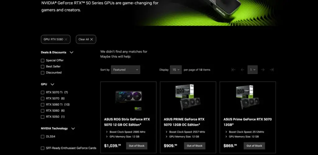
The technology industry stands on the precipice of another major shift in the graphics processing landscape as NVIDIA prepares to unveil its next generation of consumer GPUs. While the "halo" product, the GeForce RTX 5090, often captures the lion’s share of headlines for its boundary-pushing specifications, it is the GeForce RTX 5080 that many enthusiasts and professional creators are watching with the keenest interest. Positioned as the high-end workhorse of the upcoming Blackwell architecture, the RTX 5080 is expected to define the standard for 4K gaming and accelerated AI workloads for the next several years.
The transition from the current Ada Lovelace architecture to Blackwell represents more than just a routine incremental update. For NVIDIA, Blackwell is a unified effort to bridge the gap between its world-leading data center AI hardware and its consumer-facing gaming products. As rumors and leaked specifications begin to coalesce, a picture is emerging of a graphics card that seeks to balance extreme performance with the evolving demands of modern software, particularly in the realms of real-time ray tracing and generative AI.
The Blackwell Foundation and the GB203 Silicon
At the heart of the GeForce RTX 5080 lies the rumored GB203 GPU, a chip designed specifically to cater to the high-end enthusiast market. Unlike the flagship GB202, which is expected to power the RTX 5090 with a massive, near-monolithic die, the GB203 is anticipated to be a more streamlined, efficient piece of silicon. This distinction is crucial for understanding the performance tiering NVIDIA is likely to implement.
Historically, the "80-class" cards have served as the bridge between mainstream affordability and the "money-is-no-object" performance of the "90-class." With the Blackwell generation, NVIDIA appears to be doubling down on architectural efficiency. Built on a refined custom process node from TSMC—likely a specialized version of the 4N or 5nm process optimized for high-performance computing—the Blackwell chips are expected to feature a significantly higher transistor density. This allows for more CUDA cores, larger L2 caches, and more robust Ray Tracing (RT) and Tensor cores within a similar physical footprint.
The architectural improvements in Blackwell aren’t just about raw core counts. Analysts suggest that NVIDIA has overhauled the internal scheduling and execution units to better handle the asynchronous nature of modern game engines. By improving the way the GPU manages simultaneous compute and graphics tasks, the RTX 5080 could see substantial gains in frame rates even in scenarios where the CPU might otherwise become a bottleneck.
The Leap to GDDR7 Memory Technology
Perhaps the most significant hardware advancement coming with the RTX 5080 is the transition to GDDR7 memory. Since the launch of the RTX 30-series, NVIDIA has relied heavily on GDDR6X, a proprietary high-speed memory co-developed with Micron. However, as resolutions push toward 8K and textures become increasingly complex due to AI-driven asset generation, the industry has hit the limits of what GDDR6X can provide in terms of bandwidth and power efficiency.
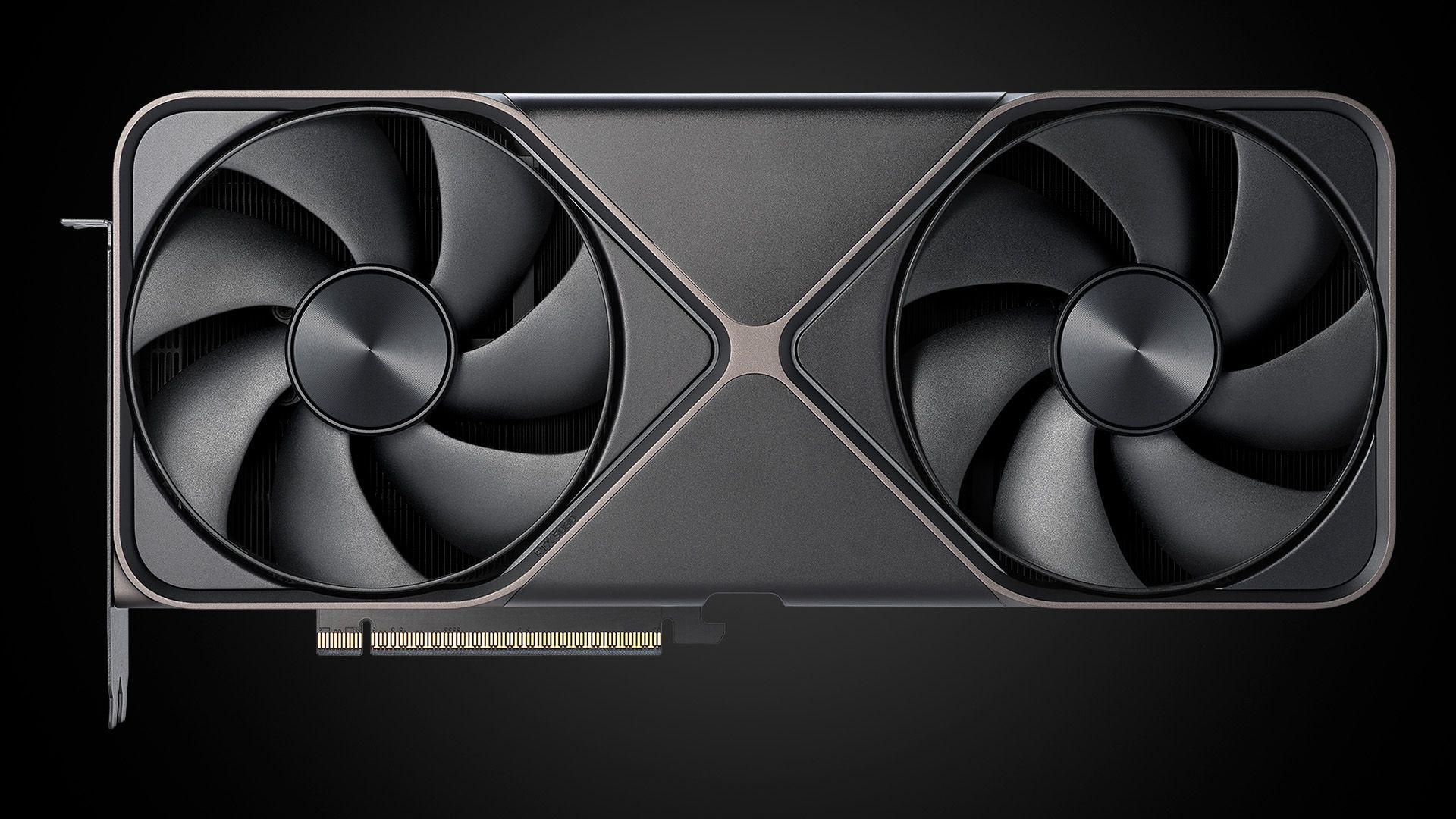
GDDR7 represents a paradigm shift in memory technology. By utilizing PAM3 (Pulse Amplitude Modulation) signaling, GDDR7 can transmit more data per clock cycle than the PAM4 or NRZ signaling used in previous generations. For the RTX 5080, this likely means a jump to memory speeds of 28Gbps or even 32Gbps. Even if NVIDIA chooses to maintain a 256-bit memory bus for the 5080—a point of much discussion among hardware trackers—the sheer speed of GDDR7 would result in a massive increase in total memory bandwidth compared to the RTX 4080.
 Hardware Reviews & PC Building
Used Hardware Purchase Leads to Unexpected Valorant Ban for German Gamer as Riot’s Vanguard Flags Secondhand CPU
The secondary market for PC components has long been a haven for...
 Hardware Reviews & PC Building
AMD Details EPYC Venice Benchmarks in Strategic Challenge to Nvidia and Intel
In a significant expansion of its data center strategy, AMD has released...
 Hardware Reviews & PC Building
Brazilian lawyers busted for attempting to manipulate court’s AI with prompt injection hidden in filing —…
The discovery was brought to public attention by Professor Vladimir Aras of...