
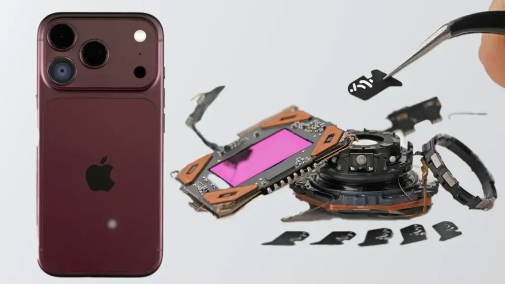
In-depth device teardowns offer an unfiltered window into the intricate engineering hidden beneath sleek glass and titanium exteriors. Following the official commercial release of Apple’s latest flagship smartphone lineup, electronics repair authority iFixit has published its comprehensive teardown of the iPhone 18 Pro and iPhone 18 Pro Max. Released simultaneously in both detailed article and video formats, the teardown provides a thorough examination of the internal architecture powering Apple’s most advanced smartphones to date. While the teardown shines a light on impressive hardware innovations—including an expanded thermal management system and a complex variable aperture camera assembly—it also highlights significant structural changes that present new challenges for independent repair technicians and hardware enthusiasts alike.
The disassembly process provides critical verification of the internal hardware differences across global variants, particularly regarding power delivery and cellular connectivity components. iFixit’s breakdown officially confirms the exact battery capacities designated for the eSIM-only iterations of the iPhone 18 Pro and iPhone 18 Pro Max. These trayless configurations are distributed across select international markets, whereas models manufactured for other regions continue to feature a traditional physical SIM card tray. The confirmation of these internal battery specs follows earlier leaks detailing the capacities of the physical SIM variants, painting a complete picture of how Apple balances internal space, power management, and regional cellular infrastructure requirements across its global supply chain.
Beyond battery specifications, the internal layout reveals notable shifts in how Apple constructs its high-end smartphones. Among the most impactful changes uncovered during the teardown is the redesigned dual-layer logic board structure, which now houses the NAND flash storage nestled deep within its sandwiched architecture. According to iFixit’s technical analysis, embedding the NAND flash memory inside the dual-layer logic board drastically complicates storage-related repairs and component-level data recovery procedures.
In prior generations, storage chips were situated in locations that, while still requiring specialized micro-soldering expertise, were considerably more accessible to advanced technicians. By placing the NAND chip between the stacked layers of the main logic board, repairing or replacing failed storage chips now requires technicians to perform a delicate board-separation process, heating and desoldering the interposer layers just to gain access to the memory module. This design choice creates a substantially higher barrier to entry for third-party repair shops, potentially rendering component-level storage repairs and data recovery efforts far less practical or economically feasible for consumers.
Repairability concerns are further compounded by an unexpected structural fragility observed during the initial display removal process. iFixit noted that during the teardown of four distinct iPhone 18 Pro units, the plastic frame supporting the screen assembly cracked or severed entirely away from the display on three of the devices. This structural cracking represents a novel issue that technicians did not encounter during disassemblies of previous iPhone generations.
When opening modern smartphones, specialized heat sources and suction tools are applied to soften the water-resistant perimeter adhesives, allowing the display to be lifted cleanly from the chassis. Under normal circumstances, the plastic sub-frame holding the display glass intact remains structural throughout this procedure. However, the recurring breakage across multiple iPhone 18 Pro units suggests a potential vulnerability in the plastic frame material, a modification in structural tolerances, or a shift in the adhesive formulation binding the screen to the chassis.
 macOS & Apple IT Support
Apple Leaks Reveal New Hardware Pipeline as $250 Million Siri AI Settlement Portal Opens
The ecosystem surrounding Apple moves at a relentless pace, with hardware leaks,...
 macOS & Apple IT Support
Apple Reverts to Soldered Storage on M6 and M5 Pro Mac Mini Models, Halving Base SSD Speeds via Single NAND Setup
Apple’s latest update to the Mac mini line brings a significant architectural...
 macOS & Apple IT Support
Apple Signals Major Smart Home Push With October 13 Announcement Featuring New Smart Display, Apple TV 4K, and HomePod mini
Apple is preparing to kick off a multi-stage autumn hardware rollout, starting...