
The deal establishes a robust, U.S.-based manufacturing source for essential advanced packaging elements, a segment of the production cycle that has historically been concentrated in East Asia. By integrating GlobalFoundries’ domestic manufacturing capabilities into TSMC’s sophisticated packaging ecosystem, the two companies are providing a pathway for technology firms to achieve a milestone that has long been sought by policymakers and industry leaders: the ability to brand their products as being entirely manufactured and packaged within the United States. This "end-to-end" American production capability is expected to be a major selling point for high-performance chips used in sensitive government applications, critical infrastructure, and cutting-edge consumer technology.
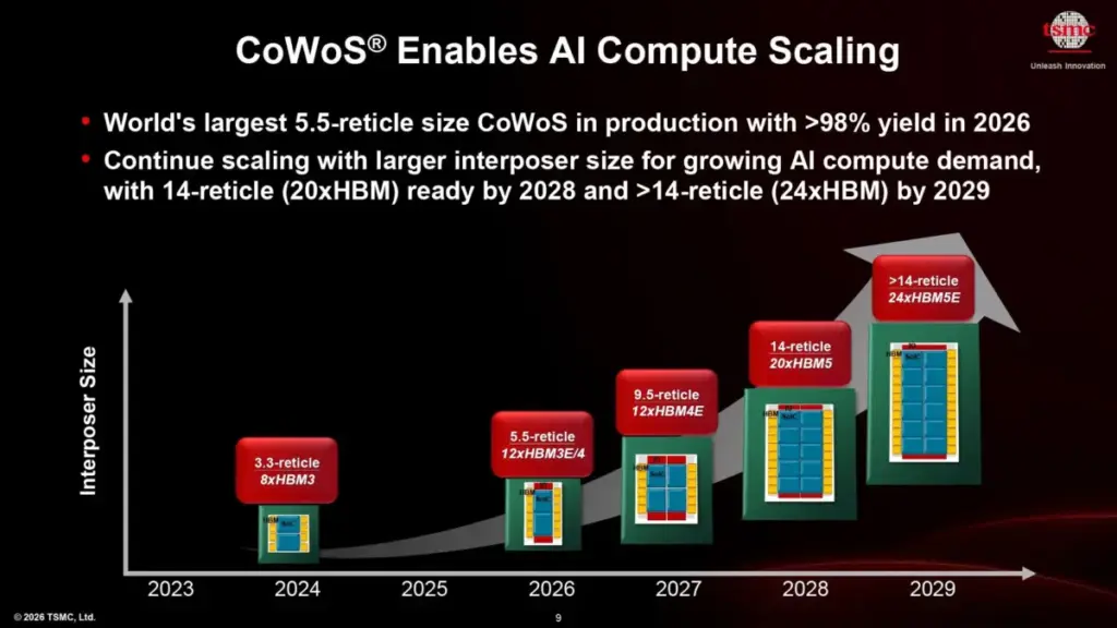
At the heart of this agreement is the silicon interposer, a sophisticated piece of technology that acts as an electrical bridge between different chips—such as a central processing unit (CPU) or a graphics processing unit (GPU) and high-bandwidth memory (HBM)—within a single package. As the semiconductor industry moves toward "chiplet" architectures, where multiple smaller chips are combined into a larger system-in-package, the role of the interposer has become paramount. These components allow for the high-speed data transfer and thermal management necessary for modern AI workloads, making them a bottleneck in the current global supply chain. By securing a massive, five-year commitment from GlobalFoundries to produce these interposers, TSMC is effectively expanding its capacity to deliver CoWoS packaging solutions, which are currently in extremely high demand due to the global explosion of generative AI and large-scale data center expansion.
The financial scale of the agreement, valued at $2 billion, underscores the long-term commitment both companies are making to this collaborative model. It is not merely a short-term solution to a capacity crunch but a foundational restructuring of how advanced packaging is sourced. The arrangement is scheduled to see volume production ramp up in the first half of 2028, reflecting the significant lead time required to qualify advanced manufacturing processes and align the complex logistics of two different foundry ecosystems. This timeline suggests that the industry is preparing for a sustained, multi-decade reliance on advanced packaging as the primary driver of semiconductor performance gains, even as traditional transistor scaling becomes increasingly difficult and expensive.
Ed Kaste, the senior vice president of CMOS Business at GlobalFoundries, highlighted the strategic importance of the deal, noting that the company’s domestic footprint is a key differentiator in the current geopolitical and economic climate. By providing manufacturing services using GlobalFoundries’ trusted U.S. manufacturing footprint, the company is creating a secure and scalable source of advanced packaging elements. Kaste emphasized that this move is designed to help customers accelerate their innovation cycles while simultaneously strengthening the semiconductor supply chain, which has faced numerous disruptions and vulnerabilities over the past several years. His comments reflect a broader industry trend toward "resilience" and "sovereignty," where the proximity and security of the manufacturing site are becoming as important as the technical specifications of the silicon itself.
The move is particularly significant for TSMC’s diverse client base, which includes some of the most influential names in the technology sector. For these clients, the ability to claim a "Made in America" status for their most advanced products carries substantial weight, not only for marketing purposes but also for navigating increasingly complex regulatory environments. In recent years, there has been a growing emphasis on the security of the semiconductor "back-end"—the packaging and testing phase—which has traditionally been the final step of production performed overseas even if the wafers themselves were fabricated in the U.S. This partnership effectively closes that loop, allowing the final, finished product to emerge from a domestic supply chain.
GlobalFoundries’ role in this partnership leverages its extensive experience in high-volume CMOS manufacturing and its established infrastructure in the United States. The company has long positioned itself as a "trusted" foundry, a designation that carries specific meaning in the context of aerospace, defense, and critical infrastructure. By applying this "trusted" framework to the production of silicon interposers for TSMC, GlobalFoundries is enabling a hybrid model of manufacturing where the world’s most advanced logic chips, often produced by TSMC, can be integrated with components made by GlobalFoundries in a secure, domestic environment.
The technical implications of this deal are as significant as the economic ones. TSMC’s CoWoS technology has become the industry standard for high-performance AI accelerators. However, the production of the silicon interposers used in CoWoS is a specialized process that requires significant cleanroom space and precise manufacturing capabilities. By outsourcing a portion of this production to GlobalFoundries, TSMC can focus its own internal capacity on the most advanced nodes and the final assembly of the CoWoS modules, while relying on GlobalFoundries to provide the essential silicon foundations. This division of labor is a pragmatic response to the sheer volume of orders currently flooding the advanced packaging market, which has outpaced the industry’s ability to build new facilities.
Furthermore, the 2028 timeline for volume production indicates that this partnership is geared toward the next generation of computing architecture. By the time production reaches scale, the industry will likely be deep into the era of "Angstrom-level" logic and even more complex 3D integration techniques. The silicon interposers produced by GlobalFoundries will need to meet rigorous standards to ensure they can support the thermal and electrical demands of these future chips. The five-year duration of the contract provides GlobalFoundries with the stability and capital certainty needed to invest in the specific equipment and process refinements required to meet TSMC’s exacting standards for CoWoS integration.
Industry analysts view this $2 billion agreement as a sign of the maturing semiconductor ecosystem, where former rivals find common ground in the face of immense technical challenges and shifting geopolitical realities. While GlobalFoundries and TSMC compete in certain segments of the foundry market, their strengths are increasingly complementary in the realm of advanced packaging. TSMC remains the undisputed leader in leading-edge logic fabrication, while GlobalFoundries has solidified its position as a leader in specialized feature-rich technologies and a critical provider of domestic manufacturing capacity. This partnership allows both companies to play to their strengths while addressing a critical gap in the U.S. semiconductor landscape.
The broader impact on the semiconductor supply chain cannot be overstated. For years, the industry has grappled with the "concentration risk" of having the majority of advanced packaging capacity located in a single geographic region. This deal represents one of the most substantial efforts to date to diversify that capacity and bring it closer to the end-markets in North America. It also serves as a model for how the industry might continue to globalize while maintaining regional security and reliability. By creating a "scalable source" of these components, as Ed Kaste noted, the partnership ensures that the sudden spikes in demand—such as those seen during the current AI boom—can be met with a more flexible and geographically distributed manufacturing base.
As the first half of 2028 approaches, the industry will be watching closely to see how the integration of GlobalFoundries’ interposers into TSMC’s CoWoS workflow progresses. The success of this collaboration could pave the way for further joint ventures and manufacturing agreements between major foundries, as the costs and complexities of semiconductor production continue to rise. For now, the $2 billion deal stands as a definitive statement on the importance of advanced packaging and the strategic value of U.S.-based manufacturing. It provides a clear roadmap for how the next generation of high-performance chips will be built, packaged, and delivered to a world increasingly hungry for computing power, all while ensuring that the supply chain remains as secure as it is innovative.
 Hardware Reviews & PC Building
Microsoft brings Snapdragon X2 Plus to 13-inch Surface Laptop, 12-inch Surface Pro — low-end systems finally get…
The introduction of the Snapdragon X2 Plus represents a substantial leap over...
 Hardware Reviews & PC Building
Tom’s Hardware Expands Digital Reach with Launch of Official Mobile Application for Android and iOS
The landscape of technology journalism has undergone a profound transformation over the...
 Hardware Reviews & PC Building
Digital Fly Brain Achieves 20 Percent Win Rate in Balatro Following Breakthrough Google Neural Mapping
In the rapidly evolving landscape of artificial intelligence and computational neuroscience, the...