
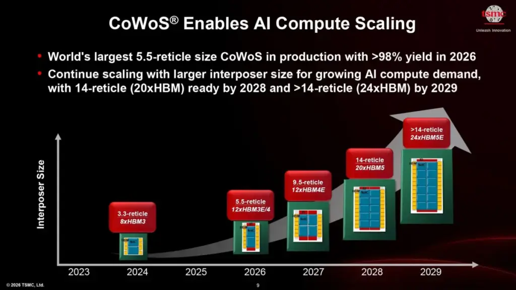
The deal establishes a robust, U.S.-based manufacturing source for essential advanced packaging elements, a segment of the production cycle that has historically been concentrated in East Asia. By integrating GlobalFoundries’ domestic manufacturing capabilities into TSMC’s sophisticated packaging ecosystem, the two companies are providing a pathway for technology firms to achieve a milestone that has long been sought by policymakers and industry leaders: the ability to brand their products as being entirely manufactured and packaged within the United States. This "end-to-end" American production capability is expected to be a major selling point for high-performance chips used in sensitive government applications, critical infrastructure, and cutting-edge consumer technology.
At the heart of this agreement is the silicon interposer, a sophisticated piece of technology that acts as an electrical bridge between different chips—such as a central processing unit (CPU) or a graphics processing unit (GPU) and high-bandwidth memory (HBM)—within a single package. As the semiconductor industry moves toward "chiplet" architectures, where multiple smaller chips are combined into a larger system-in-package, the role of the interposer has become paramount. These components allow for the high-speed data transfer and thermal management necessary for modern AI workloads, making them a bottleneck in the current global supply chain. By securing a massive, five-year commitment from GlobalFoundries to produce these interposers, TSMC is effectively expanding its capacity to deliver CoWoS packaging solutions, which are currently in extremely high demand due to the global explosion of generative AI and large-scale data center expansion.
The financial scale of the agreement, valued at $2 billion, underscores the long-term commitment both companies are making to this collaborative model. It is not merely a short-term solution to a capacity crunch but a foundational restructuring of how advanced packaging is sourced. The arrangement is scheduled to see volume production ramp up in the first half of 2028, reflecting the significant lead time required to qualify advanced manufacturing processes and align the complex logistics of two different foundry ecosystems. This timeline suggests that the industry is preparing for a sustained, multi-decade reliance on advanced packaging as the primary driver of semiconductor performance gains, even as traditional transistor scaling becomes increasingly difficult and expensive.
Ed Kaste, the senior vice president of CMOS Business at GlobalFoundries, highlighted the strategic importance of the deal, noting that the company’s domestic footprint is a key differentiator in the current geopolitical and economic climate. By providing manufacturing services using GlobalFoundries’ trusted U.S. manufacturing footprint, the company is creating a secure and scalable source of advanced packaging elements. Kaste emphasized that this move is designed to help customers accelerate their innovation cycles while simultaneously strengthening the semiconductor supply chain, which has faced numerous disruptions and vulnerabilities over the past several years. His comments reflect a broader industry trend toward "resilience" and "sovereignty," where the proximity and security of the manufacturing site are becoming as important as the technical specifications of the silicon itself.
 Hardware Reviews & PC Building
Save $250 on this award-winning Elegoo resin 3D printer with an integrated heater and 16K resolution — 39%…
The Saturn 4 Ultra is currently positioned as a flagship offering within...
 Hardware Reviews & PC Building
Amazon Prime Day 2026: Final 24 Hours of Big Deal Days Feature Massive Savings on RTX 5070 Systems, Ryzen 9800X3D, and Premium Gaming Peripherals
As the clock winds down on the 2026 iteration of Amazon’s Big...
 Hardware Reviews & PC Building
The PC gaming ray tracing obsession began with the first RTX 20 graphics cards released on this day in 2018 — the…
The debut of the GeForce 20 series was spearheaded by the release...