
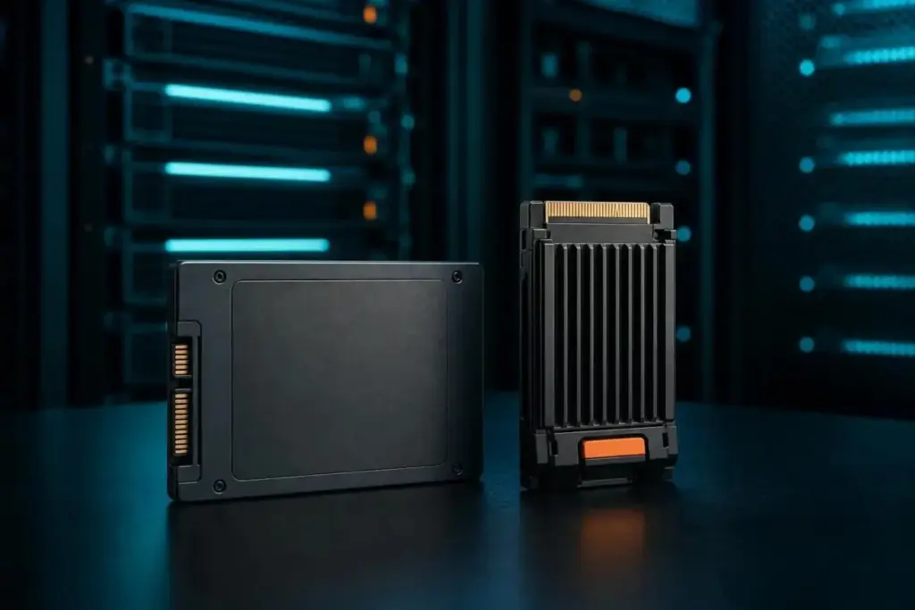
In the rapidly evolving landscape of enterprise data management, the terminology used to describe storage often becomes a source of confusion rather than clarity. For IT professionals and procurement officers, the terms "flash" and "SSD" are frequently used interchangeably, yet they represent two distinct levels of a single technology stack. To make informed purchasing decisions, one must look past the labels and understand that flash is the underlying memory technology—the electronic chips themselves—while a Solid State Drive (SSD) is the integrated device built around those chips.
As storage demands scale, the industry is moving away from the simplistic "flash versus SSD" comparison. Instead, the focus has shifted toward the specific architectural nuances that dictate performance, longevity, and cost. The real buying questions now center on NAND cell types, interface protocols, and endurance ratings. Understanding these components is essential for matching storage hardware to specific enterprise workloads, from high-frequency trading to long-term data archiving.
Flash Is the Chip, SSD Is the Product Built Around It
At its most fundamental level, flash storage refers to a specific type of non-volatile memory technology. According to industry insights from IBM, flash consists of electronic memory chips that store data without the need for moving parts. This stands in stark contrast to the mechanical nature of traditional Hard Disk Drives (HDDs). Because flash is non-volatile, it utilizes electrical charges stored on silicon to retain data even when the power is disconnected.
This inherent property of flash technology is why it is found in a vast array of devices beyond the data center. As Pure Storage notes, flash is the engine behind USB thumb drives, SD cards, smartphones, and digital cameras. However, none of these devices are considered SSDs. The distinction lies in the complexity of the implementation. An SSD is a sophisticated storage device designed to replace or augment HDDs in computing environments. It takes raw flash memory and adds a specialized controller, complex firmware, and a standardized interface.
The extra layer of intelligence provided by the controller and firmware is what separates an enterprise-grade SSD from a simple USB stick. While both use NAND flash to hold data, the SSD is engineered to handle the rigorous input/output (I/O) demands of a server or workstation, managing data placement and error correction in ways that raw flash chips cannot do on their own.
NAND vs. NOR and the Evolution of Cell Types
Flash technology is split into two primary families: NAND and NOR. The names refer to the type of logic gate used in the memory cells. IBM explains that NAND flash has become the dominant force in the storage market because it offers significantly higher storage density and faster write and erase speeds at a lower cost per bit. In contrast, NOR flash provides faster read speeds and random-access capabilities, but its lower density and higher cost have relegated it to specific roles, such as storing firmware or embedded code where execution-in-place is required.
Virtually every modern SSD is built on NAND technology. Within the world of NAND, the most critical variable for a buyer is the cell type, which determines how many bits of data are stored in each memory cell. This choice involves a direct trade-off between density, performance, and endurance.
Single-Level Cell (SLC) NAND stores just one bit per cell. As noted by Computer Compatibility, SLC is the fastest and most durable option, capable of withstanding the highest number of program/erase cycles. However, it is also the most expensive and offers the lowest density, making it rare in consumer products. It is typically reserved for mission-critical enterprise or military-grade applications where reliability is paramount.
Triple-Level Cell (TLC), storing three bits per cell, currently represents the mainstream balance for the industry, providing a sweet spot between capacity and speed. Meanwhile, Quad-Level Cell (QLC) pushes density further by storing four bits per cell. While QLC significantly lowers the cost per gigabyte and enables high-capacity drives of 4TB and beyond, it does so at the expense of write speed and long-term endurance. This makes QLC an excellent choice for read-heavy workloads but less ideal for environments with constant, heavy write operations.
What an SSD Adds Beyond the NAND Chips
The transition from a collection of raw NAND chips to a functional SSD involves the addition of a "brain" in the form of a controller. This controller is responsible for managing the inherent limitations of flash memory. Unlike magnetic storage, NAND cells wear out over time as they are written to and erased. To combat this, the controller employs wear-leveling algorithms that ensure writes are spread evenly across all available cells, preventing any single block of memory from failing prematurely.
Another critical function is garbage collection. Because NAND cannot overwrite existing data without first erasing an entire block of cells, the controller must constantly move valid data to new locations and clear out "stale" blocks to keep the drive performing efficiently. This background maintenance is invisible to the user but essential for the drive’s operation.
To support these background tasks, manufacturers utilize over-provisioning. This involves reserving a portion of the drive’s total NAND capacity—often between 7% and 28%—that is not accessible to the user. SK Hynix notes that this hidden capacity provides the controller with the "breathing room" needed to perform wear-leveling and garbage collection without impacting the drive’s advertised performance. The exact amount of over-provisioning often distinguishes a client-grade drive from an enterprise-grade model, with the latter featuring more reserved space to handle sustained, heavy workloads.
Performance is further enhanced through the use of pseudo-SLC write caches. Many TLC and QLC drives operate a small portion of their memory in a single-bit mode to act as a high-speed buffer. While this allows for extremely fast initial write speeds, Computer Compatibility points out that once this cache is exhausted during a long transfer, write speeds can drop significantly as the drive begins writing directly to the slower native NAND.
Interface, Form Factor, and the Reality of Endurance
The physical and logical connection between the SSD and the rest of the system is the next major consideration. Legacy SATA SSDs are limited by the 6 Gb/s SATA bus, which caps sequential throughput at approximately 550 MB/s. To unlock the true potential of flash, the industry moved to NVMe (Non-Volatile Memory express). NVMe allows the drive to communicate directly with the CPU over PCIe lanes, bypassing the bottlenecks of older protocols. Modern NVMe Gen 4 drives can achieve speeds between 4,500 and 7,000 MB/s, a massive leap over SATA.
It is also important to distinguish between the interface and the form factor. As IBM highlights, M.2 is a physical shape, not a speed rating. An M.2 drive can use either the SATA or NVMe protocol, though the latter is now the standard for high-performance systems. For legacy server compatibility, the 2.5-inch form factor remains common, particularly for high-capacity SATA drives.
Perhaps the most scrutinized metric in the enterprise space is endurance, usually measured in Total Bytes Written (TBW). However, TBW is not a static number. A datasheet for a high-end drive, such as the Micron 6550 ION Series, may show vastly different endurance figures depending on the workload. For example, a drive might be rated for 112,000TB of writes under a 128KB random-write test, but that figure could plummet to 28,000TB if the workload consists of smaller 4KB random writes. This discrepancy is why SK Hynix recommends that buyers carefully evaluate the warranty terms and the specific workload assumptions used by the manufacturer before committing to a purchase.
SSD vs. HDD: The One Comparison Worth Keeping
While the "Flash vs. SSD" debate is largely a matter of semantics, the "SSD vs. HDD" comparison remains a vital strategic decision. SSDs offer a radical performance advantage, with Pure Storage suggesting they can be up to 14 times faster than traditional spinning disks. They are also more resilient to physical shock and consume less power.
However, HDDs still maintain a lead in terms of cost-per-gigabyte for massive, cold-storage archives. In many enterprise environments, a hybrid approach is the most cost-effective solution. This involves using SSDs for latency-sensitive applications—such as databases and virtual desktops—while reserving HDDs for bulk data that is infrequently accessed. This tiered storage strategy allows organizations to leverage the speed of flash where it matters most without overspending on capacity for stagnant data.
The Future of Informed Storage Procurement
Ultimately, the phrase "Flash vs. SSD" is a misnomer. Flash is the ingredient, and the SSD is the finished dish. When evaluating storage solutions, the conversation should move away from these generalities and toward the technical specifications that define a drive’s behavior in a production environment.
The most effective procurement strategy involves a deep dive into the manufacturer’s datasheet. Buyers must look beyond the headline-grabbing sequential speed numbers and investigate how the drive performs when it is 80% full, how large its pseudo-SLC cache is, and what its endurance looks like under the specific block sizes used by their applications.
As the storage industry continues to mature, the gap between "best-case scenario" marketing and real-world performance remains a challenge. The only definitive way to understand how a drive will perform is to test it against the organization’s actual read/write mix. By focusing on NAND types, controller sophistication, and interface protocols rather than just the "flash" label, enterprises can build storage infrastructures that are both high-performing and economically sustainable.
 Enterprise Tech & Infrastructure
The Great Storage Divide: Navigating the Evolving Performance Landscape of SSDs and HDDs
In the modern enterprise data center, the choice between solid-state drives (SSDs)...
 Enterprise Tech & Infrastructure
Cisco Unveils Automated Control Layer to Bridge the Gap Between Isolated Quantum Nodes and Distributed Architectures
In the rapidly evolving landscape of quantum information science, the primary focus...
 Enterprise Tech & Infrastructure
The Architecture of Performance: Analyzing the Strategic Role of RAID 10 in Enterprise Storage
In the rapidly evolving landscape of enterprise data management, the selection of...