In the rapidly evolving landscape of data storage, the terms "flash" and "SSD" are frequently used interchangeably, yet they represent two distinct levels of technology. As enterprises and individual consumers navigate an era defined by massive data generation, understanding the nuance between the raw memory medium and the finished storage product has become essential for making informed purchasing decisions. While the industry often treats them as synonymous, a closer look at the engineering reveals that flash is the foundational component, while the Solid-State Drive (SSD) is the sophisticated system built around it.
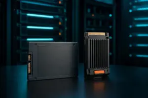
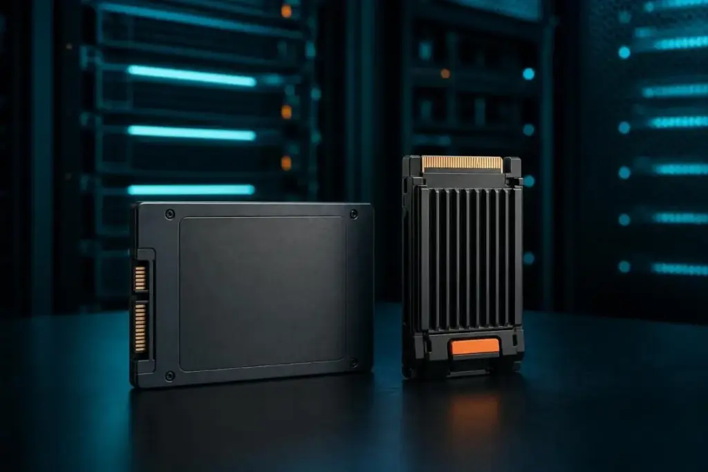
The distinction is more than academic. According to industry leaders like IBM, flash storage refers specifically to the underlying memory technology—electronic chips that store data using no moving parts. In contrast, an SSD is a comprehensive storage device that integrates these flash chips with a controller, specialized firmware, and a standardized interface to replace traditional Hard Disk Drives (HDDs). This distinction is critical because while all SSDs utilize flash memory, not all flash memory configurations qualify as SSDs.
The Foundation: Flash as the Atomic Unit of Storage
Flash storage is built upon non-volatile memory, a property that allows it to retain data even when the power supply is disconnected. This is achieved by storing electrical charges within memory cells on silicon. Because it lacks the mechanical arms and spinning platters of older technologies, flash is inherently more durable and faster than the magnetic storage of the past.
This versatility is why flash technology appears in a vast array of devices beyond computer drives. As noted by Pure Storage, the same fundamental silicon technology powers USB thumb drives, SD cards for cameras, and the internal storage of smartphones. However, a USB stick is not an SSD. The difference lies in the "extra layer" of hardware and software that manages the data. While a simple memory card might provide raw storage, an SSD includes a sophisticated controller and firmware designed to manage complex data traffic, ensure long-term reliability, and communicate with high-speed computer buses.
The technological family tree of flash splits into two primary branches: NAND and NOR. These two architectures serve very different purposes based on how their memory cells are wired. NOR flash is characterized by its ability to provide high-speed read operations and random-access capabilities, making it ideal for storing firmware and boot code where data is rarely changed but must be accessed instantly. However, NOR comes with a higher cost per bit and lower storage density.
NAND flash, on the other hand, has become the undisputed king of the storage market. It offers significantly higher storage density, smaller physical cell sizes, and much faster write and erase speeds compared to NOR. Virtually every modern SSD is built on NAND technology. Inside these chips, data is stored in floating-gate transistors that trap electrons to represent binary states. The evolution of NAND has focused almost entirely on how many bits of data can be squeezed into a single cell, leading to the various "tiers" of memory that consumers see on spec sheets today.
The Spectrum of NAND: SLC, TLC, and QLC
For a buyer, the most impactful variable inside a NAND chip is the cell type, which dictates the balance between speed, endurance, and price. Single-Level Cell (SLC) NAND stores only one bit per cell. Because the controller only needs to distinguish between two electrical states (on or off), SLC is incredibly fast and durable, capable of enduring tens of thousands of write cycles. However, because it is the least dense, it is also the most expensive. Computer Compatibility notes that SLC is rarely found in consumer products, instead being reserved for mission-critical enterprise servers or military-grade equipment where failure is not an option.
 Enterprise Tech & Infrastructure
The Unprecedented Ascent of the Global Server Market: A Vertical Climb into the AI Era
There is a specific, visceral sensation associated with watching an F-18A Hornet...
 Enterprise Tech & Infrastructure
The Security Architecture of Enterprise Storage: Evaluating the Vulnerabilities of DAS and NAS Systems
In the modern enterprise landscape, data is frequently characterized as the lifeblood...
 Enterprise Tech & Infrastructure
Navigating the Shift to Software-Defined Storage: Essential Strategies for Modern Enterprise Data Management
The landscape of enterprise data management is undergoing a fundamental transformation as...