

The trajectory of the modern datacenter has, for the past decade, been defined by an unrelenting drive toward architectural complexity. This evolution is not a result of engineering for engineering’s sake, but rather a necessary response to the diversifying demands of global compute workloads. As the industry shifts from general-purpose virtualization toward the intensive requirements of agentic AI, high-performance computing (HPC), and massive-scale cloud infrastructure, the hardware underlying these services must become more specialized.
AMD today marked a significant milestone in this journey with the official launch of its sixth-generation Epyc processor family, codenamed "Venice." This new generation represents more than just an incremental update; it is a comprehensive overhaul of the Epyc platform designed to widen the performance gap between AMD and its traditional X86 rival, Intel, while simultaneously fortifying its position against the growing collective of Arm-based custom silicon providers.
The Venice rollout is characterized by an unprecedented level of choice and technical distinction. For the first time, AMD is deploying two different server sockets, two distinct I/O dies, and two variations of compute dies to populate its initial product line. The launch includes 31 different CPU stock keeping units (SKUs), ranging from entry-level 8-core processors to a massive 256-core flagship. These parts cover a power envelope spanning 130 watts to 600 watts, with pricing that scales from a modest $700 to $14,904 per unit when purchased in high-volume 1,000-unit trays.
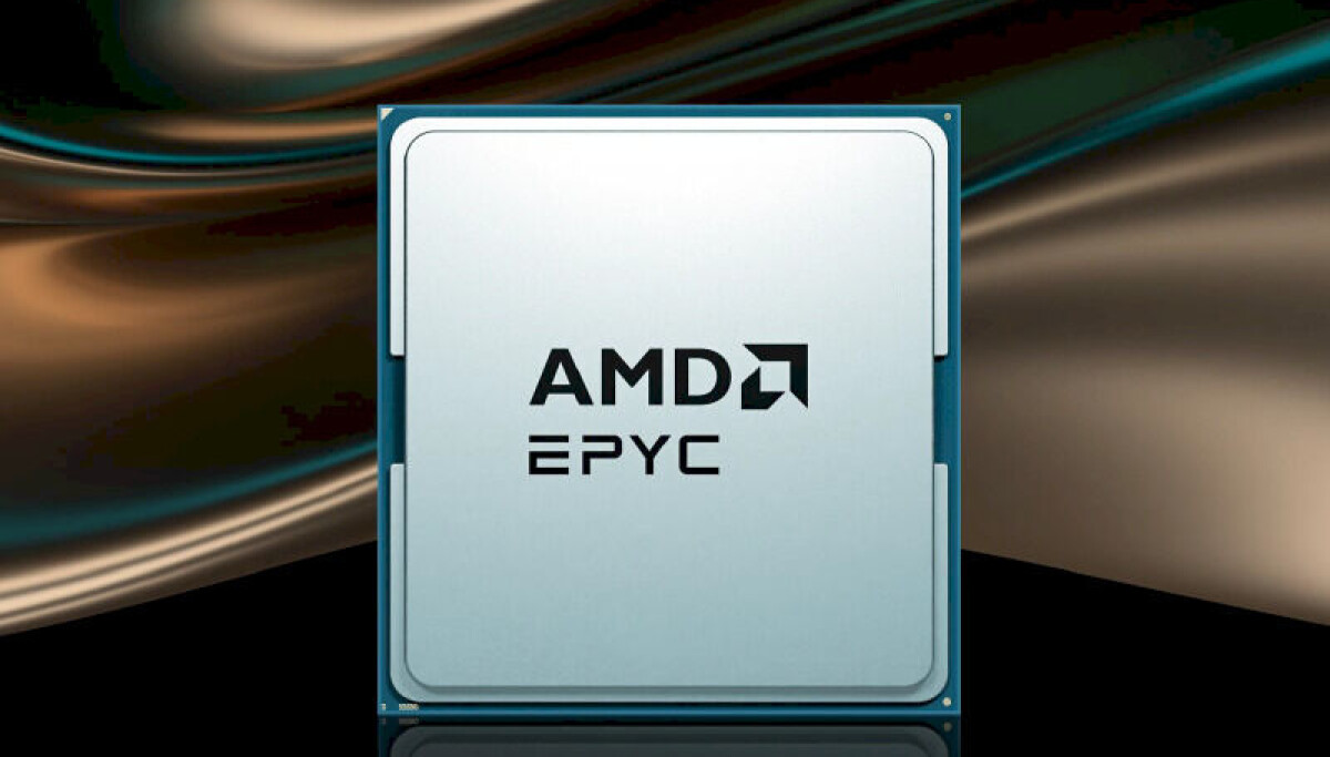
The Architecture of Venice: Blurring the Lines Between Efficiency and Performance
At the heart of the Venice generation lies the Zen 6 core architecture. In previous generations, such as "Genoa" and "Turin," AMD maintained a sharp distinction between its standard Zen cores and its "c" or compact cores. The Zen 5c cores, for instance, were optimized for density by halving the L3 cache per core compute die (CCD), which allowed for higher core counts but often penalized performance in cache-sensitive applications.
With Venice, AMD has shifted its strategy. The company is now blurring the distinction between the standard Zen 6 and the compact Zen 6c cores. The cache hierarchies remain consistent across the two designs, ensuring that the compact variants do not suffer the same performance penalties as their predecessors. Instead, the differentiation is handled through the optimization of internal schedulers. One version is tuned for massive core density and lower clock speeds, while the other is optimized for higher frequencies in lower-core-count configurations.
This architectural harmony is supported by cutting-edge manufacturing. Both the 12-core CCD, which features 48 MB of L3 cache, and the 32-core CCD, equipped with 128 MB of L3 cache, are manufactured using Taiwan Semiconductor Manufacturing Co.’s (TSMC) advanced 2-nanometer process. This move to 2nm represents a significant leap in transistor density and power efficiency, allowing AMD to pack 256 cores into a single package without the thermal runaway that would have plagued older process nodes.
Conversely, the I/O and memory dies (IOD) for the Venice line are etched using TSMC’s 6-nanometer process. This remains a pragmatic engineering choice. As signaling and I/O components do not scale or shrink as effectively as compute logic, using the most advanced nodes for these parts offers diminishing returns. By staying on a mature 6nm process for the IOD, AMD can manage costs and ensure signal integrity while focusing its most expensive silicon budget on the compute dies where the performance gains are most impactful.
 Enterprise Tech & Infrastructure
Understanding the Architecture of Modern Storage: The Nuances Between Flash Memory and Solid-State Drives
In the rapidly evolving landscape of data management, the terminology used to...
 Enterprise Tech & Infrastructure
Upscale AI Unveils SkyHammer Fabric to Challenge Nvidia’s Dominance in Scale-Up AI Networking
The history of high-performance computing has long been defined by a tension...
 Enterprise Tech & Infrastructure
Decoding the Amazon S3 Bill: Why the Per-Gigabyte Rate Is Often the Smallest Part of Cloud Storage Costs
In the world of enterprise cloud infrastructure, the Amazon S3 storage bill...