
The trajectory of the modern datacenter has, for the past decade, been defined by an unrelenting drive toward architectural complexity. This evolution is not a result of engineering for engineering’s sake, but rather a necessary response to the diversifying demands of global compute workloads. As the industry shifts from general-purpose virtualization toward the intensive requirements of agentic AI, high-performance computing (HPC), and massive-scale cloud infrastructure, the hardware underlying these services must become more specialized.
AMD today marked a significant milestone in this journey with the official launch of its sixth-generation Epyc processor family, codenamed "Venice." This new generation represents more than just an incremental update; it is a comprehensive overhaul of the Epyc platform designed to widen the performance gap between AMD and its traditional X86 rival, Intel, while simultaneously fortifying its position against the growing collective of Arm-based custom silicon providers.
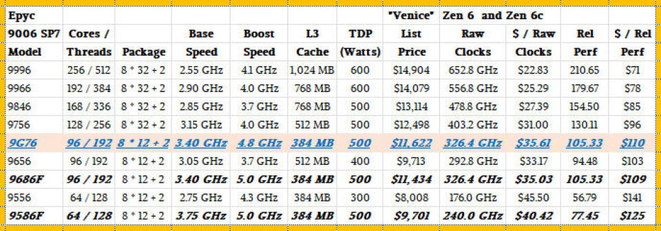
The Venice rollout is characterized by an unprecedented level of choice and technical distinction. For the first time, AMD is deploying two different server sockets, two distinct I/O dies, and two variations of compute dies to populate its initial product line. The launch includes 31 different CPU stock keeping units (SKUs), ranging from entry-level 8-core processors to a massive 256-core flagship. These parts cover a power envelope spanning 130 watts to 600 watts, with pricing that scales from a modest $700 to $14,904 per unit when purchased in high-volume 1,000-unit trays.
The Architecture of Venice: Blurring the Lines Between Efficiency and Performance
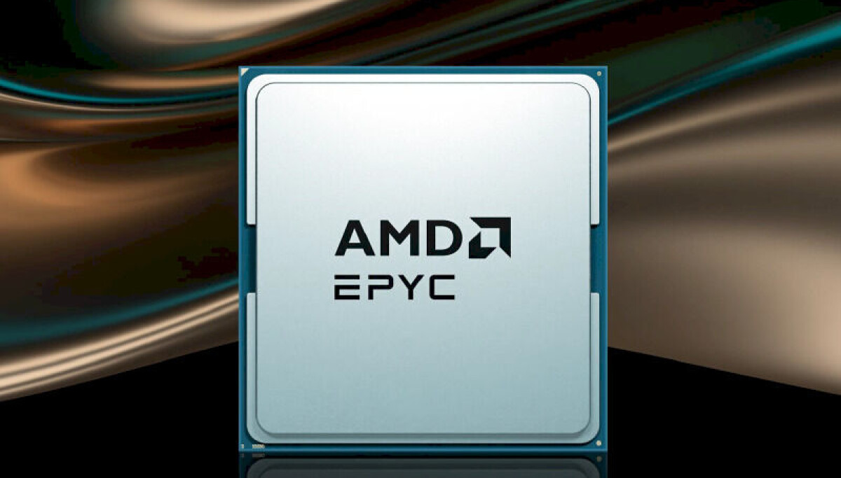
At the heart of the Venice generation lies the Zen 6 core architecture. In previous generations, such as "Genoa" and "Turin," AMD maintained a sharp distinction between its standard Zen cores and its "c" or compact cores. The Zen 5c cores, for instance, were optimized for density by halving the L3 cache per core compute die (CCD), which allowed for higher core counts but often penalized performance in cache-sensitive applications.
With Venice, AMD has shifted its strategy. The company is now blurring the distinction between the standard Zen 6 and the compact Zen 6c cores. The cache hierarchies remain consistent across the two designs, ensuring that the compact variants do not suffer the same performance penalties as their predecessors. Instead, the differentiation is handled through the optimization of internal schedulers. One version is tuned for massive core density and lower clock speeds, while the other is optimized for higher frequencies in lower-core-count configurations.
This architectural harmony is supported by cutting-edge manufacturing. Both the 12-core CCD, which features 48 MB of L3 cache, and the 32-core CCD, equipped with 128 MB of L3 cache, are manufactured using Taiwan Semiconductor Manufacturing Co.’s (TSMC) advanced 2-nanometer process. This move to 2nm represents a significant leap in transistor density and power efficiency, allowing AMD to pack 256 cores into a single package without the thermal runaway that would have plagued older process nodes.
Conversely, the I/O and memory dies (IOD) for the Venice line are etched using TSMC’s 6-nanometer process. This remains a pragmatic engineering choice. As signaling and I/O components do not scale or shrink as effectively as compute logic, using the most advanced nodes for these parts offers diminishing returns. By staying on a mature 6nm process for the IOD, AMD can manage costs and ensure signal integrity while focusing its most expensive silicon budget on the compute dies where the performance gains are most impactful.
A Tale of Two Sockets: SP7 and SP8
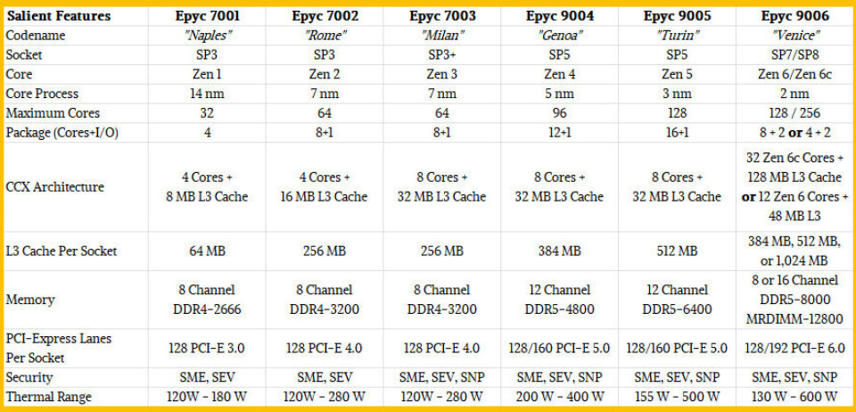
The Venice generation introduces a dual-socket strategy to address different segments of the market. The SP7 socket is the heavyweight of the lineup, designed for the most demanding throughput and AI-centric tasks. It utilizes a pair of I/O dies that support a staggering 16 channels of DDR5 memory. When paired with Multi-Ranked DIMMs (MRDIMMs) running at 12.8 GT/sec, the SP7 platform can deliver up to 1.6 TB/sec of memory bandwidth. Even with standard RDIMMs at 8 GT/sec, the platform provides 1 TB/sec of bandwidth.
Connectivity on the SP7 is equally robust, offering 96 lanes of PCI-Express 6.0 running at 64 Gb/sec, supplemented by eight lanes of PCI-Express 4.0. In dual-socket configurations, the platform exposes 128 PCI-Express 6.0 lanes to the system, with another 64 lanes dedicated to the NUMA (Non-Uniform Memory Access) link that maintains coherency between the two processors.
The nine initial Venice chips designed for the SP7 socket include the top-tier 256-core models. Notable among these is the Epyc 9G76, a specialized part designed specifically for Helion AI racks. While similar in architecture to the HPC-focused Epyc 9686F, the 9G76 is positioned for hyperscalers and cloud builders who require massive parallelization for agentic AI workloads.
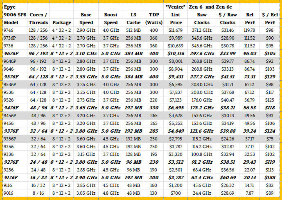
For the mainstream enterprise market, AMD offers the SP8 socket. These processors are intended for more traditional datacenter roles where extreme core density is less critical than balanced I/O and cost-efficiency. The SP8 socket supports eight DDR5 memory channels per socket and provides 128 PCI-Express 6.0 lanes. Interestingly, while the SP8 has half the memory bandwidth of the SP7, it offers 33 percent more I/O lanes in a single-socket configuration. In a two-socket setup, the SP8 platform can expose 192 PCI-Express 6.0 lanes to the outside world.
The SP8 variants of the Venice line, comprising 22 different SKUs, are scheduled to begin shipping in the first half of 2027. This staggered release allows AMD to prioritize the high-margin, high-demand AI and HPC sectors with the SP7 socket before filling out the rest of the enterprise stack.
Performance Gains and the Historical Perspective
To understand the magnitude of the Venice launch, it is necessary to look back at the history of the Epyc line and its predecessor, the Opteron. AMD’s internal benchmarks and architectural analysis indicate a 20 percent improvement in instructions per clock (IPC) for the Zen 6 core over the Zen 5 core for integer workloads. This is a substantial generational jump, particularly given the already high baseline established by the "Turin" processors.
When Venice is compared to the "Shanghai" quad-core Opteron processors launched in late 2008—the last competitive Opteron line before Intel’s Nehalem architecture took the lead—the progress is staggering. The flagship Epyc 9996, designed for the SP7 socket, offers approximately 190 times the performance of the top-bin Opteron 2393 SE from the Great Recession era.
The economic story is just as compelling. While the price of a top-bin chip has risen roughly 12.8 times over that period, the cost per unit of performance has plummeted. The Epyc 9996 provides a price-to-performance ratio that is nearly 15 times better than the Shanghai Opteron. This dramatic improvement in "bang for the buck" has been the primary engine driving server consolidation over the last decade, allowing enterprises to replace racks of older equipment with a single Venice-based server.
The performance curve across the Epyc generations—from Naples (7001 series) to Rome, Milan, Genoa, and Turin—has been largely linear. However, the 256-core Venice SP7 parts represent a significant upward inflection point. By doubling down on core count and memory bandwidth, AMD is pushing the throughput of a single socket into territory previously reserved for multi-node clusters.
The Competitive Landscape
AMD’s aggressive positioning with Venice is a direct challenge to Intel’s latest Xeon offerings, but it is also a defensive move against the "Arm collective." Hyperscalers like Amazon, Google, and Microsoft have increasingly turned to their own custom Arm-based silicon to power their internal workloads and cloud instances. By offering a massive 256-core X86 part that maintains software compatibility while matching or exceeding the density of Arm designs, AMD is providing a powerful reason for these cloud giants to remain within the X86 ecosystem.
The pricing strategy for Venice reflects this competitive reality. While AMD is charging a premium for the SP8 mainstream versions—which feature fewer cores running at higher clock speeds—the SP7 throughput-oriented parts are priced to maximize value for high-density deployments. This tiered approach ensures that AMD can compete on raw speed for frequency-sensitive enterprise applications while dominating on throughput for the scale-out workloads of the AI era.
As the industry moves toward 2027, the Venice generation of Epyc processors stands as a testament to AMD’s ability to execute a complex, multi-year roadmap. By successfully navigating the transition to 2nm manufacturing and diversifying its platform with the SP7 and SP8 sockets, AMD has ensured that its sixth generation of Epyc will remain the touchstone for datacenter performance for years to come. The heat is not just on Intel; it is rising across the entire semiconductor landscape, and AMD appears more than ready to meet the challenge.
 Enterprise Tech & Infrastructure
Decoding the True Cost of Amazon S3: Why Storage Class Rates Are Only Half the Story
For enterprise IT leaders and cloud architects, the promise of Amazon S3...
 Enterprise Tech & Infrastructure
Bridging the Storage Divide: The Strategic Role of Fibre Channel over Ethernet in Modern Data Centers
In the complex landscape of enterprise data management, the tension between high-performance...
 Enterprise Tech & Infrastructure
The Evolution of the Data Center: Understanding the Rise and Role of Hyperconverged Storage
In the rapidly shifting landscape of enterprise technology, the traditional silos of...