In the rapidly evolving landscape of data storage, the terms "flash" and "SSD" are frequently used interchangeably, yet they represent two distinct levels of technology. As enterprises and individual consumers navigate an era defined by massive data generation, understanding the nuance between the raw memory medium and the finished storage product has become essential for making informed purchasing decisions. While the industry often treats them as synonymous, a closer look at the engineering reveals that flash is the foundational component, while the Solid-State Drive (SSD) is the sophisticated system built around it.
The distinction is more than academic. According to industry leaders like IBM, flash storage refers specifically to the underlying memory technology—electronic chips that store data using no moving parts. In contrast, an SSD is a comprehensive storage device that integrates these flash chips with a controller, specialized firmware, and a standardized interface to replace traditional Hard Disk Drives (HDDs). This distinction is critical because while all SSDs utilize flash memory, not all flash memory configurations qualify as SSDs.
The Foundation: Flash as the Atomic Unit of Storage
Flash storage is built upon non-volatile memory, a property that allows it to retain data even when the power supply is disconnected. This is achieved by storing electrical charges within memory cells on silicon. Because it lacks the mechanical arms and spinning platters of older technologies, flash is inherently more durable and faster than the magnetic storage of the past.
This versatility is why flash technology appears in a vast array of devices beyond computer drives. As noted by Pure Storage, the same fundamental silicon technology powers USB thumb drives, SD cards for cameras, and the internal storage of smartphones. However, a USB stick is not an SSD. The difference lies in the "extra layer" of hardware and software that manages the data. While a simple memory card might provide raw storage, an SSD includes a sophisticated controller and firmware designed to manage complex data traffic, ensure long-term reliability, and communicate with high-speed computer buses.
The technological family tree of flash splits into two primary branches: NAND and NOR. These two architectures serve very different purposes based on how their memory cells are wired. NOR flash is characterized by its ability to provide high-speed read operations and random-access capabilities, making it ideal for storing firmware and boot code where data is rarely changed but must be accessed instantly. However, NOR comes with a higher cost per bit and lower storage density.
NAND flash, on the other hand, has become the undisputed king of the storage market. It offers significantly higher storage density, smaller physical cell sizes, and much faster write and erase speeds compared to NOR. Virtually every modern SSD is built on NAND technology. Inside these chips, data is stored in floating-gate transistors that trap electrons to represent binary states. The evolution of NAND has focused almost entirely on how many bits of data can be squeezed into a single cell, leading to the various "tiers" of memory that consumers see on spec sheets today.
The Spectrum of NAND: SLC, TLC, and QLC
For a buyer, the most impactful variable inside a NAND chip is the cell type, which dictates the balance between speed, endurance, and price. Single-Level Cell (SLC) NAND stores only one bit per cell. Because the controller only needs to distinguish between two electrical states (on or off), SLC is incredibly fast and durable, capable of enduring tens of thousands of write cycles. However, because it is the least dense, it is also the most expensive. Computer Compatibility notes that SLC is rarely found in consumer products, instead being reserved for mission-critical enterprise servers or military-grade equipment where failure is not an option.
Triple-Level Cell (TLC) has become the mainstream standard for the modern PC market. By storing three bits per cell, it offers a pragmatic balance of high capacity and reasonable performance. Most high-end consumer NVMe drives utilize TLC to provide the speeds required for gaming and professional video editing without the prohibitive costs of SLC.
At the budget-friendly end of the spectrum lies Quad-Level Cell (QLC). By packing four bits into every cell, QLC drives achieve massive capacities at lower price points, often showing up in 4TB models and above. The trade-off, however, is a reduction in write speeds and overall lifespan. Because the controller must precisely manage sixteen different voltage levels within a single transistor to read four bits of data, the process is slower and more taxing on the hardware. This makes QLC ideal for "read-heavy" workloads—such as storing a massive library of movies or games—but less suitable for "write-heavy" environments like database logging.
The Controller: The Brain of the SSD
If NAND chips are the "storage bins," the controller is the "warehouse manager." This is the component that truly transforms raw flash into an SSD. A stack of NAND chips on its own is relatively "dumb" and prone to rapid degradation. The controller provides the intelligence necessary to keep the drive functioning over several years.
Two of the most critical tasks handled by the controller and its firmware are wear-leveling and garbage collection. NAND cells have a finite lifespan; they can only be written to and erased a certain number of times before they lose the ability to hold a charge. Wear-leveling ensures that the controller spreads data writes evenly across all available cells, preventing any single block of memory from wearing out prematurely. Garbage collection is a background process that reclaims memory blocks containing "stale" data that has been deleted by the operating system, ensuring that the drive always has clean blocks ready for new information.
To support these maintenance tasks, manufacturers employ "over-provisioning." This involves reserving a portion of the drive’s total NAND capacity—often between 7% and 28%—that remains invisible to the user. This extra space acts as a buffer for the controller to move data around during wear-leveling and garbage collection. According to SK Hynix, higher grades of SSDs typically feature more over-provisioning to sustain consistent performance under heavy workloads.
Performance is further enhanced through pseudo-SLC caching. Many TLC and QLC drives treat a small portion of their capacity as if it were SLC (writing only one bit per cell) to provide a burst of high speed. While this allows for impressive "headline" speeds in marketing materials, Computer Compatibility warns that once this cache is filled during a long file transfer, write speeds will drop significantly to the drive’s native, slower rate.
Interface, Form Factor, and the Reality of Endurance
The physical and logical connection between the SSD and the computer is the final piece of the puzzle. For years, the SATA interface was the standard, but it is now a bottleneck. Capped at roughly 550 MB/s, SATA was designed for the era of spinning hard drives. The modern successor is NVMe (Non-Volatile Memory Express), which allows the SSD to communicate directly with the CPU via PCIe lanes. A Gen 4 NVMe drive can reach speeds of 7,000 MB/s, more than ten times the limit of SATA.
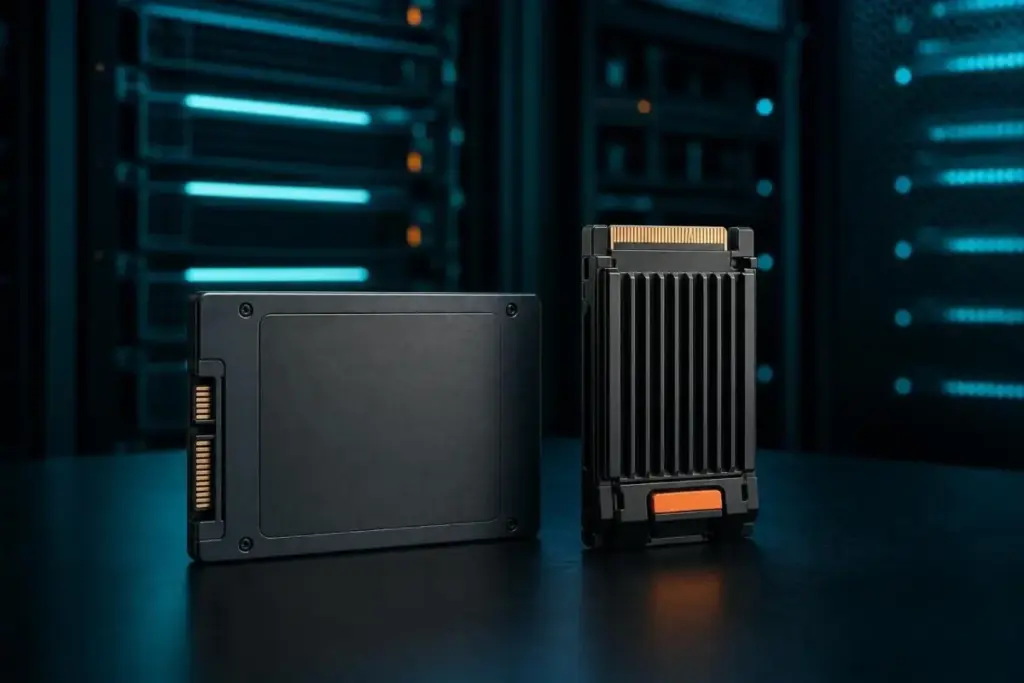
It is important to distinguish these protocols from the physical form factor. M.2 is a shape—a small, gum-stick-sized card—but an M.2 slot can support either SATA or NVMe depending on the motherboard and the drive. Conversely, the traditional 2.5-inch brick shape is almost exclusively used for SATA drives today.
When evaluating the lifespan of these devices, the industry uses a metric called Total Bytes Written (TBW). This figure represents the amount of data a user can write to the drive before the warranty expires or the NAND is expected to fail. However, TBW is not a fixed constant. Micron’s data for the 6550 ION series demonstrates that endurance varies wildly based on the "block size" of the data being written. A drive might be rated for 112,000TB of endurance when writing large 128KB blocks of data, but that rating could plummet to 28,000TB if the workload consists of small 4KB random writes. This discrepancy occurs because smaller, random writes cause more "write amplification," where the controller must move more internal data to accommodate the new information.
The Role of the HDD in a Flash-Dominated World
Despite the dominance of SSDs, the Hard Disk Drive (HDD) has not been rendered obsolete. The comparison between the two remains a matter of physics and economics. SSDs are circuit-based and offer near-instant access times, with Pure Storage claiming they can be up to 14 times faster than HDDs. However, HDDs still win on the metric of cost-per-gigabyte.
For massive data archives, "cold" storage, or secondary backups where speed is not a priority, the spinning magnetic platter remains the more cost-effective choice. Many enterprise environments utilize hybrid storage strategies, placing active, latency-sensitive data on NVMe SSDs while relegating bulk data to high-capacity HDDs.
Final Considerations for the Strategic Buyer
The transition from asking "Flash vs. SSD" to asking about specific NAND types and interfaces marks a maturation in how we approach technology. For the modern buyer, the checklist for a new drive should move beyond simple capacity.
One must consider the NAND type (TLC for performance, QLC for value), the interface (NVMe for speed, SATA for legacy compatibility), and the endurance rating (TBW) relative to the intended workload. Furthermore, performance should be viewed through the lens of drive fullness. SK Hynix suggests that performance can degrade once a drive reaches 80% capacity, as the controller has fewer free blocks to perform its essential maintenance.
Ultimately, the most reliable way to gauge a drive’s suitability is to look past the peak performance numbers on the box. Real-world utility is found in the manufacturer’s datasheet, specifically in the fine print regarding block sizes and sustained write speeds. In a world where data is the most valuable commodity, understanding the distinction between the chip and the device is the first step toward building a reliable digital infrastructure.
 Enterprise Tech & Infrastructure
AMD Reports Record Datacenter Growth in Third Quarter as AI Demand Reshapes the Competitive Landscape
In the volatile ecosystem of global technology, capitalism thrives on the friction...
 Enterprise Tech & Infrastructure
The Hidden Complexity of Cloud Storage: Decoding the Real Drivers of Amazon S3 Expenditures
For many enterprise IT departments, the monthly Amazon Web Services (AWS) bill...
 Enterprise Tech & Infrastructure
Navigating the Hidden Financial Mechanics of Amazon S3: Strategies for Enterprise Cost Optimization
In the landscape of modern enterprise cloud architecture, Amazon S3 has long...