In the rapidly evolving landscape of data storage, terms like "Flash" and "SSD" are frequently used interchangeably by consumers and enterprise procurement teams alike. However, as data demands reach unprecedented levels and the underlying silicon technology becomes increasingly complex, the distinction between these two concepts has become a critical focal point for understanding hardware performance. Industry experts and major technology providers, including IBM, Pure Storage, and SK Hynix, are emphasizing that the real conversation is no longer about choosing between Flash and SSDs, but rather understanding how Flash technology is harnessed within the architecture of a Solid-State Drive to meet specific workload requirements.
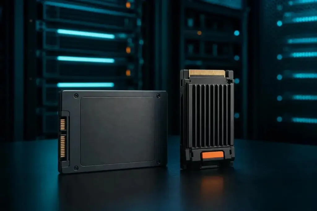
At its most fundamental level, Flash storage refers to the memory technology itself. These are the electronic, non-volatile memory chips that store data without the need for moving parts. An SSD, by contrast, is a complete, sophisticated storage device built around those Flash chips. To use an analogy common in hardware circles, Flash is the engine, while the SSD is the entire vehicle, complete with a transmission, fuel management system, and a driver’s interface. Understanding this distinction is the first step in decoding the technical specifications that determine whether a drive will thrive in a high-transaction database environment or serve as a budget-friendly backup solution.
Flash Is the Chip, SSD Is the Product Built Around It
The core of the distinction lies in the physical and logical structure of the hardware. According to technical insights from IBM, Flash storage is defined by its non-volatile nature, meaning it retains data through electrical charges trapped in memory cells on silicon even when the power is disconnected. This property is why Flash technology is found in a vast array of devices beyond computer storage drives, including smartphones, digital cameras, and SD cards.
However, a raw Flash chip is not inherently capable of functioning as a primary storage drive for a modern computer. As Pure Storage notes, the transition from a simple chip to a Solid-State Drive requires an integrated "extra layer" consisting of a controller, specialized firmware, and a standardized interface. While a USB thumb drive or an SD card utilizes Flash memory, they lack the complex controller logic and high-speed interfaces required to be classified as an SSD. It is within this architectural layer—the controller and firmware—where the most meaningful differences between enterprise-grade and consumer-grade drives are found. The controller acts as the "brain" of the device, managing how data is written, moved, and protected, which ultimately dictates the drive’s reliability and speed.
The Evolution of NAND and the Trade-Offs of Cell Density
The Flash memory used in modern storage is generally divided into two families: NAND and NOR. These names refer to the type of logic gate used in the storage cells. IBM explains that NOR Flash is characterized by its ability to provide fast read speeds and random-access capabilities, making it ideal for storing firmware and embedded code that must be accessed quickly. However, NOR is expensive and lacks the storage density required for high-capacity drives.
This is why virtually every modern SSD is built on NAND Flash. NAND offers significantly higher storage density, smaller physical cell sizes, and faster write and erase speeds, all at a lower cost per bit. Within the world of NAND, the most critical variable for a buyer is the cell type, which refers to how many bits of data are stored in a single transistor cell. This is a game of precision and physics: the more bits stored per cell, the more voltage levels the controller must be able to distinguish, which directly impacts performance and longevity.
Computer Compatibility identifies three primary tiers of NAND used today. Single-Level Cell (SLC) stores only one bit per cell. It is the fastest, most durable, and most expensive option, but because of its low density, it has largely disappeared from the consumer market, finding its home in military-grade and high-end enterprise systems where failure is not an option. Triple-Level Cell (TLC), storing three bits per cell, has become the mainstream standard, offering a balanced middle ground of speed, capacity, and durability. Finally, Quad-Level Cell (QLC) stores four bits per cell. While QLC allows for massive capacities at a lower price point—often seen in budget drives and high-capacity 4TB or 8TB models—it trades away write speed and endurance to achieve those gains.
 Enterprise Tech & Infrastructure
Navigating the Hidden Complexities of Amazon S3: Strategies for Mitigating Enterprise Storage Overspend
The financial architecture of cloud storage is often more complex than it...
 Enterprise Tech & Infrastructure
The Shift to Software-Defined Excellence: Understanding the Rise and Impact of Hyperconverged Storage
The landscape of enterprise data management is undergoing a fundamental transformation as...
 Enterprise Tech & Infrastructure
Upscale AI Challenges Nvidia’s Scale-Up Dominance with SkyHammer Fabric and $2 Billion Valuation
For decades, the world’s leading CPU manufacturers have maintained a fiercely proprietary...