
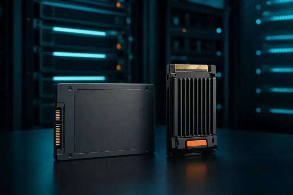
In the rapidly evolving landscape of enterprise data management, the terminology used to describe storage solutions often leads to a fundamental misunderstanding among procurement officers and IT professionals. Two of the most frequently conflated terms are "flash" and "SSD." While often used interchangeably in marketing literature, they represent two distinct levels of technology: one is a raw material, and the other is a finished industrial product. As data centers transition away from legacy spinning media, understanding the interplay between these two—and the specific configurations of the NAND chips inside them—has become a prerequisite for building efficient, high-performance infrastructure.
The distinction is straightforward but critical. Flash storage refers to the underlying memory technology itself—specifically, electronic memory chips that store data on silicon without the need for moving parts. In contrast, a Solid State Drive (SSD) is a complete, integrated storage device. It is an architecture built around flash memory chips, incorporating a sophisticated controller, specialized firmware, and a standardized physical interface designed to replace traditional Hard Disk Drives (HDDs). According to industry insights from IBM, flash is defined by its non-volatile nature; it stores data as electrical charges within memory cells. Because it requires no moving components, it is inherently more resilient and faster than the magnetic platters of the past. This non-volatile property allows flash to retain data even when the power is disconnected, which is why the technology is ubiquitous not only in enterprise servers but also in consumer electronics like smartphones, cameras, and USB thumb drives.
However, as Pure Storage points out, a USB stick or an SD card, while utilizing flash technology, does not qualify as an SSD. The defining characteristic of an SSD is the "intelligence" layered on top of the raw NAND chips. This includes the controller and firmware that manage how data is distributed, as well as the interface that allows the drive to communicate with the rest of the system. This distinction is where the real complexity of modern storage begins, as the performance and longevity of a drive are determined less by the fact that it uses "flash" and more by the specific type of NAND and the quality of the controller managing it.
The Internal Mechanics: NAND, NOR, and the Hierarchy of Cells
To understand why some SSDs cost significantly more than others, one must look at the specific family of flash memory used within the device. Flash memory generally splits into two primary families: NAND and NOR. As IBM explains, these two types serve very different roles in the computing ecosystem. NOR flash is characterized by its ability to provide fast read speeds and random-access capabilities, but it suffers from high per-bit costs and slower write and erase speeds. Consequently, NOR is rarely used for bulk storage, instead finding its home in firmware and embedded systems where small amounts of code must be accessed quickly.
The vast majority of modern SSDs are built on NAND flash. NAND offers a superior balance of high storage density, smaller physical cell size, and significantly faster write and erase cycles, all at a lower cost. Within a NAND chip, data is stored in floating-gate transistors that trap electrons to represent binary states. However, not all NAND is created equal. The industry categorizes NAND based on how many bits of data are stored in each individual memory cell, a factor that dictates the drive’s speed, endurance, and price.
At the top of the hierarchy is Single-Level Cell (SLC) NAND, which stores only one bit per cell. Computer Compatibility notes that SLC is the fastest and most durable version of flash, capable of withstanding the highest number of write cycles. Because of its high manufacturing cost and lower density, it is almost never found in consumer-grade hardware. Instead, SLC is reserved for mission-critical enterprise applications and military-grade storage where failure is not an option.
For most mainstream enterprise and consumer applications, the industry relies on Triple-Level Cell (TLC) NAND, which stores three bits per cell. TLC represents the current "sweet spot" in the market, offering a pragmatic balance of capacity, performance, and durability. For budget-conscious deployments or high-capacity models—typically those reaching 4TB and above—manufacturers utilize Quad-Level Cell (QLC) NAND. By storing four bits per cell, QLC achieves much higher density and a lower cost per gigabyte, but this comes at the expense of write speeds and overall longevity. This makes QLC ideal for read-heavy workloads but less suitable for environments with constant, high-volume data writes.
 Enterprise Tech & Infrastructure
Securing the Data Core: Evaluating the Security Architectures of DAS and NAS in the Enterprise
In the modern enterprise landscape, data is frequently described as the new...
 Enterprise Tech & Infrastructure
The Great Storage Divide: Navigating the Evolving Performance Landscape of SSDs and HDDs
In the modern enterprise data center, the choice between solid-state drives (SSDs)...
 Enterprise Tech & Infrastructure
Upscale AI Challenges Nvidia’s Dominance with SkyHammer Scale-Up Fabric and Unified AI Networking
The history of the semiconductor industry is littered with the remains of...