
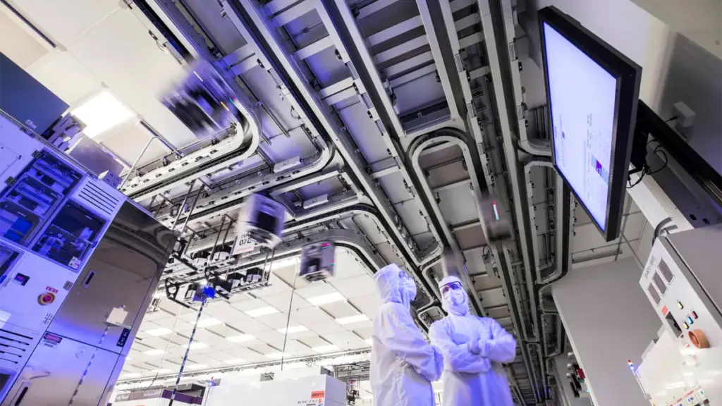
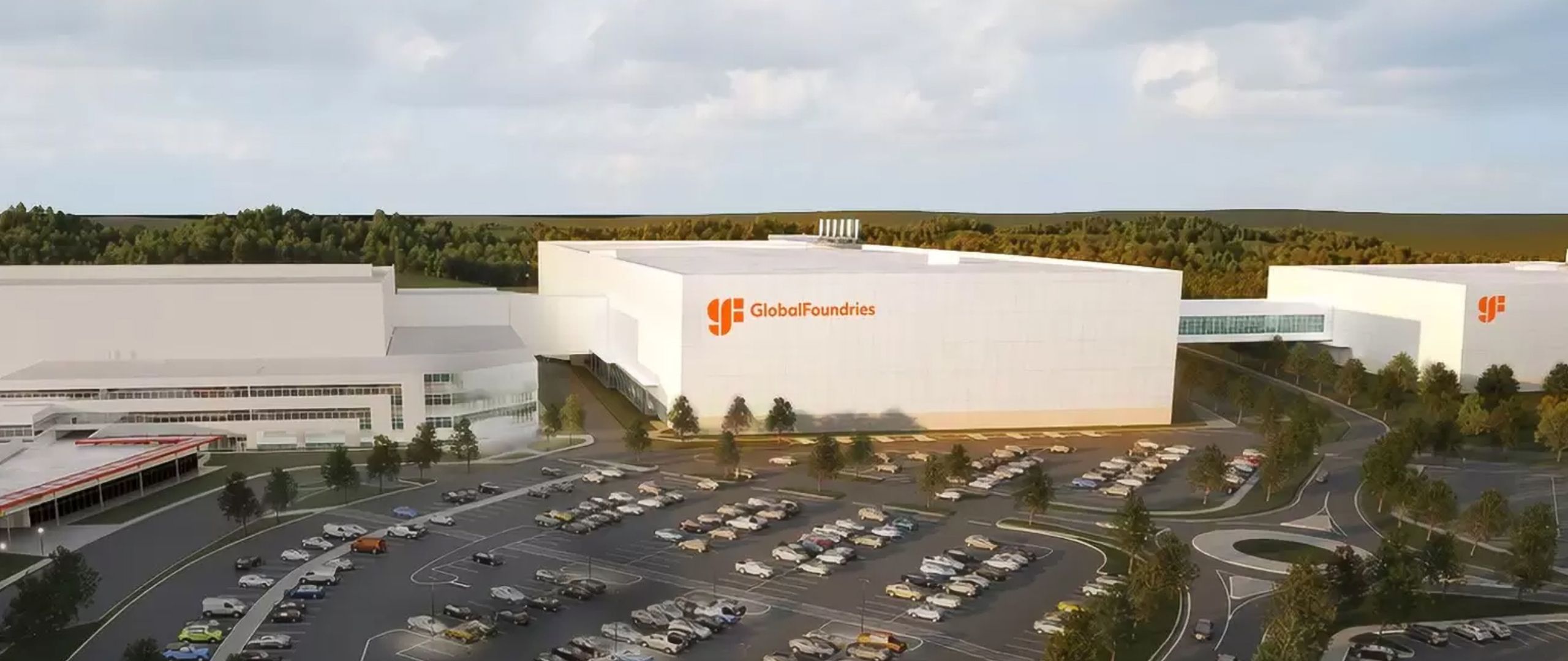
By designing FDX Fusion to work with existing Deep Ultraviolet (DUV) immersion lithography, GlobalFoundries is positioning itself as a cost-effective alternative for companies that need 7nm-level performance but cannot justify the high "entry fee" of EUV-based designs. This approach relies on advanced multi-patterning techniques and the inherent physical advantages of the FD-SOI structure to hit performance targets.
The decision to stick with DUV also has significant implications for manufacturing yields and cycle times. Because the industry has decades of experience with DUV, the processes are well-understood, and the equipment is already installed in many of GlobalFoundries’ existing fabs. This allows for a more predictable ramp-up to high-volume manufacturing and reduces the technical hurdles associated with the "stochastic" defects often found in early-stage EUV production.
The Persistence of Planar Transistors
The semiconductor industry largely moved away from planar (flat) transistors when it transitioned from 28nm to 16nm/14nm, adopting the 3D FinFET (Fin Field-Effect Transistor) structure to overcome short-channel effects. However, FDX Fusion aims to prove that planar transistors still have a future at the "leading-edge" of specialized nodes.
Planar transistors offer several distinct advantages over FinFETs, particularly in the realm of RF and analog integration. Because they are flat, they exhibit lower parasitic capacitance, which is vital for high-frequency communication chips used in 5G and the upcoming 6G standards. Furthermore, FD-SOI’s planar structure allows for "back-biasing," a technique where a voltage is applied to the substrate to dynamically adjust the transistor’s threshold voltage. This allows a chip to switch between a "high-performance mode" and an "ultra-low-power mode" on the fly, a feat that is much more difficult to achieve with FinFETs.
By keeping the architecture planar, GlobalFoundries also simplifies the design process for its customers. The design rules for FinFET nodes are notoriously complex and restrictive, often requiring significant engineering resources to navigate. A planar 7nm-class node could theoretically offer a more "user-friendly" design environment for chip architects, potentially shortening the time-to-market for new products.
Target Markets and the 2030 Horizon
GlobalFoundries is targeting a 2030 window for high-volume manufacturing (HVM) of FDX Fusion. While this timeline may seem distant compared to the rapid-fire releases of the consumer electronics world, it aligns perfectly with the development cycles of the industries GlobalFoundries serves.
 Hardware Reviews & PC Building
Russian Military Targets Ukrainian Data Centers in Widening Campaign Against Digital Infrastructure
The Russian military has initiated a series of targeted strikes against critical...
 Hardware Reviews & PC Building
PsiQuantum Leverages Quantum Silicon Photonics to Transform AI Data Center Networking with High-Efficiency Optical Switching
In a strategic move that highlights the growing convergence between quantum computing...
 Hardware Reviews & PC Building
Frontier Model Forum Introduces Standardized Jailbreak Rating Framework to Address Evolving AI Cybersecurity Threats
The rapid evolution of generative artificial intelligence has brought with it a...