In the rapidly evolving landscape of artificial intelligence, the hardware that powers the world’s most sophisticated models is undergoing a fundamental shift. It is no longer enough to simply produce faster, more powerful chips; the industry is now moving toward highly specialized configurations designed to match specific, increasingly complex workloads. Google, a pioneer in custom silicon, is doubling down on this philosophy by introducing two significant new variants of its Tensor Processing Unit (TPU) accelerators. These new entries, the "Sunfish" TPU 8t and "Zebrafish" TPU 8i, represent a strategic refinement of the hardware Google first teased earlier this year, aiming to optimize everything from massive frontier model training to the high-frequency demands of agentic AI inference.
These upcoming accelerators, which are slated for a gradual rollout starting next year, are designed to serve both Google’s internal research needs and its growing base of Google Cloud customers. While Google remains its own best customer—using these machines to develop the next generations of its Gemini models—the company is also paving the way for direct customers to eventually harness this homegrown compute power within their own data centers. However, the road from announcement to availability is a long one, often dictated by the complex physics of chip fabrication and the logistical challenges of global data center deployment.
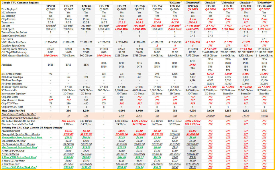
The two new variants are essentially specialized versions of the TPU 8 architecture revealed in April. The TPU 8t, shepherded through the design and production process by Broadcom’s chip unit, is currently making its way into Google’s data centers. Meanwhile, the TPU 8i, which involves a partnership with MediaTek, has faced some developmental delays, leaving its current shipping status somewhat opaque. Industry analysts expect the modified versions of these Sunfish and Zebrafish systems to begin their installation phase in early 2027. If current trends hold, a ramp-up period would follow, likely extending through mid-2028 before these machines are widely available across multiple Google Cloud regions.
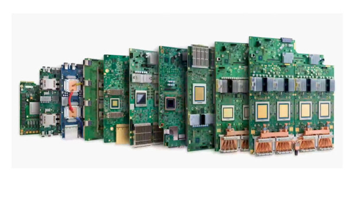
To understand the timeline for such a massive infrastructure project, one only needs to look at the history of the TPU v7p, codenamed "Ironwood." First deployed for Google’s internal use in late 2025, it took approximately a year for the company to build enough excess capacity to offer the Ironwood accelerators for rent on the public cloud. Today, pricing for Ironwood is active in regions like US-Central1 in Iowa and Europe-West2 near London, highlighting the significant lag between the birth of a chip and its commercial accessibility.
At the heart of Google’s training strategy is the TPU 8t (Sunfish). This device is explicitly engineered for the Herculean task of AI training. It utilizes Google’s proprietary 3D torus interconnect, a networking topology that allows for a shared coherent memory space spanning up to 9,600 accelerators. This configuration is capable of delivering an extraordinary 121 exaflops of performance at FP4 precision. Each individual Sunfish device is equipped with 216 GB of HBM3E memory distributed across six stacks, providing what is arguably the largest shared memory footprint in the current AI sector. This massive memory overhead is essential for training "frontier" models like Gemini, which require enormous amounts of data to be processed simultaneously.
Mark Lohmeyer, vice president and general manager of AI and computing infrastructure at Google, recently detailed how these machines are being deployed. The 9,600-unit pods are ganged together to form clusters exceeding one million TPU 8t devices. It was this level of unprecedented scale that allowed Google to train its Gemini 4 Carbon model. While the development of Gemini 4 Carbon faced some internal delays, its release on October 28 marked a significant milestone, outperforming its predecessor, Gemini 4 Argon, across various benchmarks. For those accessing these models via API, Google has set introductory pricing at $2 per million input tokens and $10 per million output tokens, with substantial discounts for cached inputs.
However, training is only one side of the AI coin. As models move from the laboratory to the real world, the focus shifts to inference—the process of using a trained model to generate responses or perform tasks. This is where the TPU 8tx comes in. While it retains the core compute power of the 8t, the 8tx is optimized for the low-latency requirements of inference, particularly for "agentic" workloads where multiple inference streams may be running concurrently to perform complex, multi-step tasks.
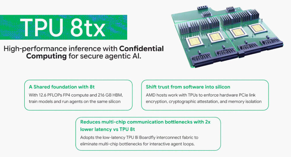
The most notable change in the TPU 8tx is the replacement of the 3D torus interconnect with a "boardfly" topology. This is a variant of the dragonfly interconnect designed by Google to create a more tightly coupled system. By reducing the pod size from 9,600 accelerators to 1,152, Google has effectively flattened the network. This reduction in the fabric’s diameter results in an average latency that is roughly half that of the 3D torus configuration.
Furthermore, the TPU 8tx introduces a surprising shift in the host processor. Google has opted to replace its own Arm-based Axion CPU with an unnamed AMD Epyc processor for this specific variant. This decision appears to be driven by security requirements. The AMD Epyc chips feature specialized on-board root of trust and encryption accelerators. This allows data to remain encrypted until the exact moment it is processed by the TPU, and to be re-encrypted immediately afterward. While Google has its own security processors, the integration of these features into the AMD silicon provides a ready-made solution for high-security inference tasks. Industry observers speculate whether this move to AMD is a temporary measure until Google can integrate similar encryption features into its next generation of Axion and TPU 9 architectures.
On the more efficiency-focused side of the spectrum is the TPU 8i Max (Zebrafish). This variant is designed to tackle large-context AI inference, where the model needs to "remember" or process vast amounts of information in a single session. To achieve this, Google has doubled the number of Zebrafish accelerator complexes per socket. However, the memory configuration reveals a complex set of architectural trade-offs.
While the original Zebrafish 8i chip featured 288 GB of HBM3 memory, the TPU 8i Max utilizes two chips, each with only 192 GB of capacity. Although the total memory per socket has increased, the amount of memory per unit of compute has actually decreased by about 33 percent. This suggests that Google is spreading its HBM3 allocation across more chips to create a larger aggregate shared memory footprint for things like Key-Value (KV) caches, which are vital for maintaining context in long conversations. This approach risks leaving some compute power "stranded"—meaning the chip has more processing ability than it has memory to support—but for large-context inference, memory capacity is often the more critical bottleneck.
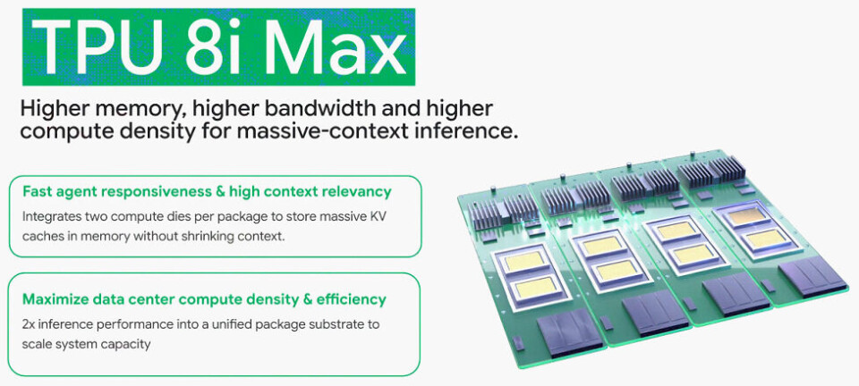
The physical design of the TPU 8i Max also hints at further innovations. Observations of the hardware show a different Inter-Chip Interconnect (ICI) port at the bottom of the board compared to other TPU 8 variants, though Google has yet to provide a detailed technical explanation for this change.
Pricing for these new units remains speculative, but the market expects Google to maintain a tiered structure. Training-focused units like the TPU 8t will likely command a premium, as the industry’s hunger for frontier model training remains insatiable. Conversely, inference-focused chips like the 8i and 8i Max will likely be priced to encourage high-volume token generation.
Beyond the hardware, Google is also introducing a sophisticated software layer known as TPU Sync. This hierarchical storage management system is designed to maximize the efficiency of HBM memory, particularly during the "bursty" nature of agentic AI workloads. In many agentic scenarios, a TPU may sit idle while an AI agent "thinks" or waits for a response from another part of the system. TPU Sync addresses this inefficiency by moving working memory off the TPU chip when an agent pauses and restoring it instantly when processing resumes.
Lohmeyer explained that this software orchestration allows Google to apply those freed-up resources to other tasks, significantly driving up system utilization. By maximizing the work done by each chip, Google aims to lower the cost per transaction and the overall cost of running complex AI activities. Because TPU Sync is a software-based solution, Google is backporting it to previous generations, including the TPU v5 through v8.
As the industry moves toward 2027, the deployment of these specialized Sunfish and Zebrafish variants will likely define Google’s ability to compete in a market where the efficiency of inference is becoming just as important as the raw power of training. By diversifying its TPU lineup, Google is signaling that the future of AI infrastructure lies in precision engineering—building the right tool for the right job, rather than a one-size-fits-all solution.
 Enterprise Tech & Infrastructure
The Evolution of the Data Center: How Hyperconverged Storage is Redefining Enterprise Infrastructure
In the rapidly evolving landscape of enterprise technology, the transition from hardware-centric...
 Enterprise Tech & Infrastructure
IBM, AMD, and Oak Ridge National Laboratory Launch Integrated Co-Design Platform to Accelerate Quantum Error Correction
The pursuit of fault-tolerant quantum computing has long been defined by a...
 Enterprise Tech & Infrastructure
Upscale AI Challenges Nvidia’s Dominance with SkyHammer Scale-Up Fabric
For decades, the architecture of high-performance computing has been defined by a...