

The transition from the Maia 200 to the Maia 300 involves a fundamental shift in both manufacturing and architecture. While the Maia 100 and 200 were monolithic designs produced on TSMC’s 5-nanometer and 3-nanometer processes respectively, the Clea Maia 300 moves to a sophisticated chiplet architecture utilizing TSMC’s 2-nanometer N2P process. The Clea package is less a single chip and more a "system in a socket," comprising seven distinct chips and eight High Bandwidth Memory (HBM) stacks on an interposer. By breaking out I/O and HBM controllers from the compute and SRAM cache elements, Microsoft can optimize each component individually. For instance, while the compute tiles leverage the cutting-edge 2nm process, the I/O and memory controller dies likely utilize a more mature 5nm process to maintain yield and performance without unnecessary cost.
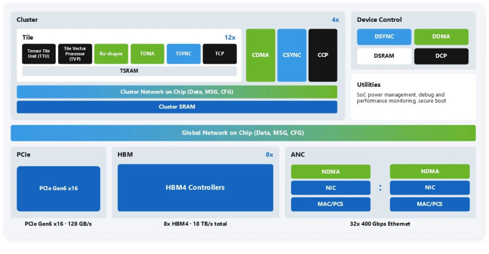
The internal organization of the Maia 300 consists of four tile clusters, with each cluster containing twelve compute tiles. These tiles feature a Tile Tensor Unit (TTU) and a Tile Vector Processor (TVP), supported by a Tile Data Movement Engine (TDMA) and a Tile Control Processor (TCP). Microsoft has also integrated two specific elements first introduced in the Maia 200: a reshaper and a tile synchronizer. These components are critical for managing dataflow across the entire system, ensuring that information moves efficiently from the network down to the individual compute tiles.
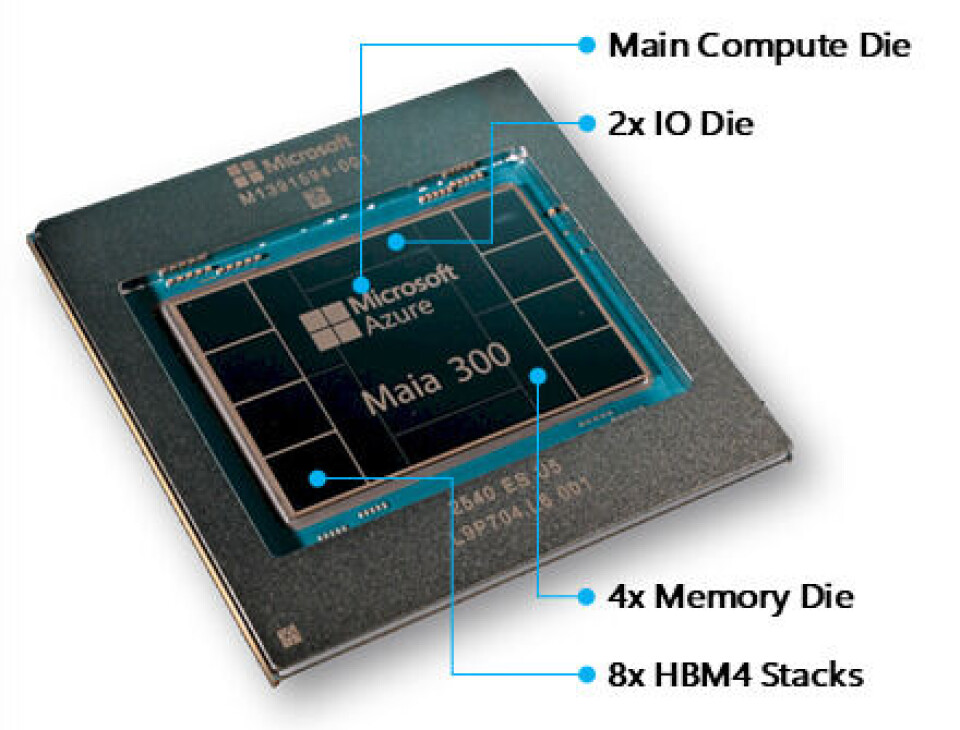
Memory architecture is another area where the Maia 300 pushes the envelope. The device features 288 GB of HBM4, likely sourced from SK Hynix, providing roughly 18 TB/sec of bandwidth. This is balanced by a massive aggregate SRAM bandwidth of approximately 166.2 TB/sec across the complex. Interestingly, Microsoft has adopted a "NUMA-ish" memory approach for Clea. Instead of sharing all HBM memory across all compute tiles globally, pairs of compute tiles are tied to specific HBM4 memory banks. This localized memory access is designed to accelerate specific routines essential for generative AI inference, a design choice also mirrored in other high-end AI accelerators like OpenAI’s rumored "Jalapeno" chip.
The networking capabilities of the Maia 300 are equally ambitious. Microsoft has introduced the second generation of its custom AI Transport Layer (ATL 2.0), a custom RoCE (RDMA over Converged Ethernet) implementation. The networking strategy for Maia has evolved with every generation. The original Maia 100 used 400 Gb/sec links to create a coherency domain of 2,304 XPUs. The Maia 200 expanded this to 6,144 devices. With the Maia 300, Microsoft is leveraging a more efficient 1U form factor and advanced liquid cooling to double the density of its racks.
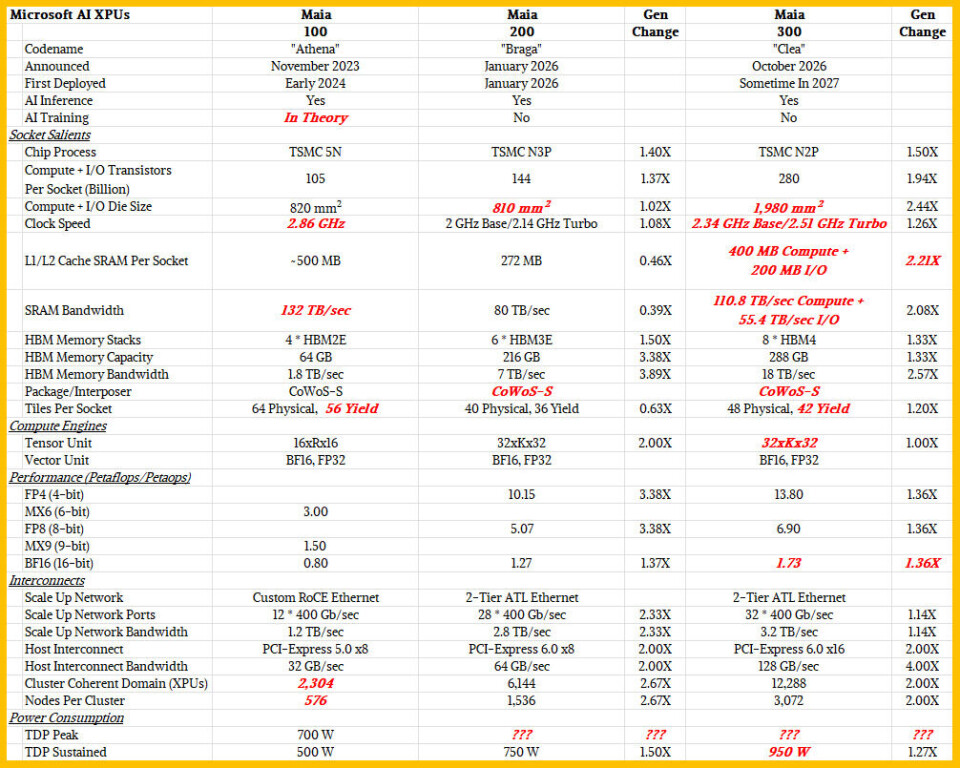
A standard Maia 300 rack now houses 96 XPUs across two dozen servers, compared to the 48 XPUs found in Maia 200 racks. By lashing 128 of these racks together, Microsoft can create a single coherency domain of 12,288 accelerators. This is currently the largest coherency domain reported by any major cloud provider, significantly exceeding the 72 or 144 GPU domains offered by Nvidia and AMD in their rack-scale systems. Even Google’s forthcoming "Sunfish" TPU 8t training chip is expected to top out at 9,600 units in a single domain. This massive scale is intended to allow the Maia 300 system to behave as a single, giant computer, capable of handling the most complex agentic AI workflows with minimal latency.
 Enterprise Tech & Infrastructure
Understanding Fibre Channel over Ethernet: Bridging the Gap Between High-Performance Storage and Ethernet Ubiquity
In the rapidly evolving landscape of data center infrastructure, the quest for...
 Enterprise Tech & Infrastructure
The Unprecedented Ascent of the Global Server Market: A Vertical Climb into the AI Era
There is a specific, visceral sensation associated with watching an F-18A Hornet...
 Enterprise Tech & Infrastructure
Navigating the Hidden Complexities of Amazon S3 Cost Management
For many enterprise IT departments, the monthly Amazon Web Services (AWS) bill...